Monocrystalline silicon piece washing device

A technology for single crystal silicon wafers and cleaning devices, applied in cleaning methods and appliances, cleaning methods using liquids, chemical instruments and methods, etc., capable of solving the problems of residual stains on the surface of single crystal silicon wafers, poor cleaning quality, and cleaning Time-consuming and labor-intensive problems, to achieve the effect of saving time and labor, high degree of cleaning automation, and high cleaning quality

Inactive Publication Date: 2017-07-18
杭州泰扶新能源有限公司
View PDF6 Cites 8 Cited by
  • Summary
  • Abstract
  • Description
  • Claims
  • Application Information

AI Technical Summary

Problems solved by technology

[0003] The present invention solves the problems such as residual stains on the surface of the single crystal silicon wafer when the existing single crystal silicon wafer is cleaned with a cleaning device, or the cleaning device used has a cleaning device design during the cleaning process. Poor rationality, low cleaning efficiency, time-consuming and labor-intensive cleaning, poor cleaning quality and other current conditions provide a more effective and thorough cleaning to remove residual dirt and chipping on the surface of single crystal silicon wafers, with high cleaning efficiency. The cleaning is more time-saving and labor-saving, the cleaning quality is improved, and the cleaning device design is more reasonable.

Method used


Image

  • Monocrystalline silicon piece washing device
  • Monocrystalline silicon piece washing device

Examples


Embodiment Construction

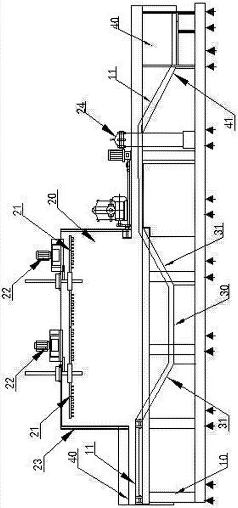
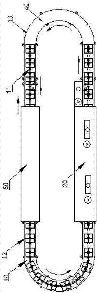
[0016] figure 1 , figure 2 In the shown embodiment, a single crystal silicon wafer cleaning device includes a cleaning tank and an annular cleaning frame. A conveying track 11 is installed on the annular cleaning frame 10, and a plurality of single crystal wafers are installed on the conveying track. The silicon wafer conveying bracket 12, the conveying track 11 includes a conveying straight path, a conveying ramp connected to the conveying straight path, and an annular conveying path at both ends of the ring-shaped cleaning rack, and a cleaning chamber 20 is installed on the straight section of the ring-shaped cleaning rack. , the ring-shaped cleaning rack is provided with a drying chamber 50 at another straight line section, and a plurality of inclined sinking cleaning tanks 30 are installed in the cleaning chamber, and the conveying track 11 is transported through the cleaning chamber 20, and in the tank in the inclined sinking cleaning tank 30 The conveying track has a c...


PUM


Abstract

The invention discloses a single crystal silicon wafer cleaning device. A conveying track is arranged on a circular frame, and a plurality of single crystal silicon wafer conveying brackets are arranged on the conveying track. The conveyor inclined channel and the circular conveyor at both ends of the ring frame are equipped with a cleaning room and a drying room on the straight section of the ring frame. Each end is equipped with an inclined wave section in the tank; the top of the cleaning room is provided with a plurality of upper spray pipes that can be adjusted up and down above the inclined wave section of the inner conveyance, and there are multiple rings at one end of the ring frame. End inclined sinking cleaning tank, multiple inclined sinking cleaning tanks and the bottom of multiple ring end inclined sinking cleaning tanks are equipped with ultrasonic cleaning structure and heating structure; more effective and thorough cleaning to remove surface residues of single crystal silicon wafers No dirt and flakes, high cleaning efficiency, time-saving and labor-saving cleaning, high cleaning quality.

Description

technical field [0001] The invention relates to a single crystal silicon wafer production device, in particular to a single crystal wafer cleaning device used in the single crystal silicon wafer production process. Background technique [0002] Monocrystalline silicon wafers must be cleaned during production to avoid device failure due to contamination. The purpose of cleaning is to remove surface organic or inorganic contamination impurities. At present, when most manufacturers clean monocrystalline silicon wafers, either there are likely to be residual stains on the surface of monocrystalline silicon wafers, etc., or the cleaning devices used have problems in the cleaning process. The design of the cleaning device is reasonable. Poor performance, low cleaning efficiency, time-consuming and laborious cleaning, poor cleaning quality and effect. Contents of the invention [0003] The present invention solves the problems such as residual stains on the surface of the singl...

Claims


Application Information

Patent Timeline
Patent Type & Authority Applications(China)
IPC IPC(8): B08B3/04B08B3/08B08B3/12B08B3/10B08B13/00
CPCB08B3/04B08B3/08B08B3/10B08B3/12B08B13/00B08B2203/007
Inventor 曹建鸿
Owner 杭州泰扶新能源有限公司
Why Eureka
Try Eureka