

Device for disassembling electrostatic chuck
An electrostatic chuck and mounting hole technology, which is applied in the field of semiconductors, can solve the problems of O-ring 5 with large and limited adhesion, uneven pulling force, etc., and achieve the effect of improving efficiency
- Summary
- Abstract
- Description
- Claims
- Application Information
AI Technical Summary
Problems solved by technology
Method used
Image

Examples
Embodiment Construction
[0032] In order to make the above objects, features and advantages of the present invention more obvious and understandable, the technical solutions in the embodiments of the present invention will be clearly and completely described below in conjunction with the drawings in the embodiments of the present invention. Apparently, the described embodiments are only some of the embodiments of the present invention, but not all of them. Based on the embodiments of the present invention, all other embodiments obtained by persons of ordinary skill in the art without creative efforts fall within the protection scope of the present invention.
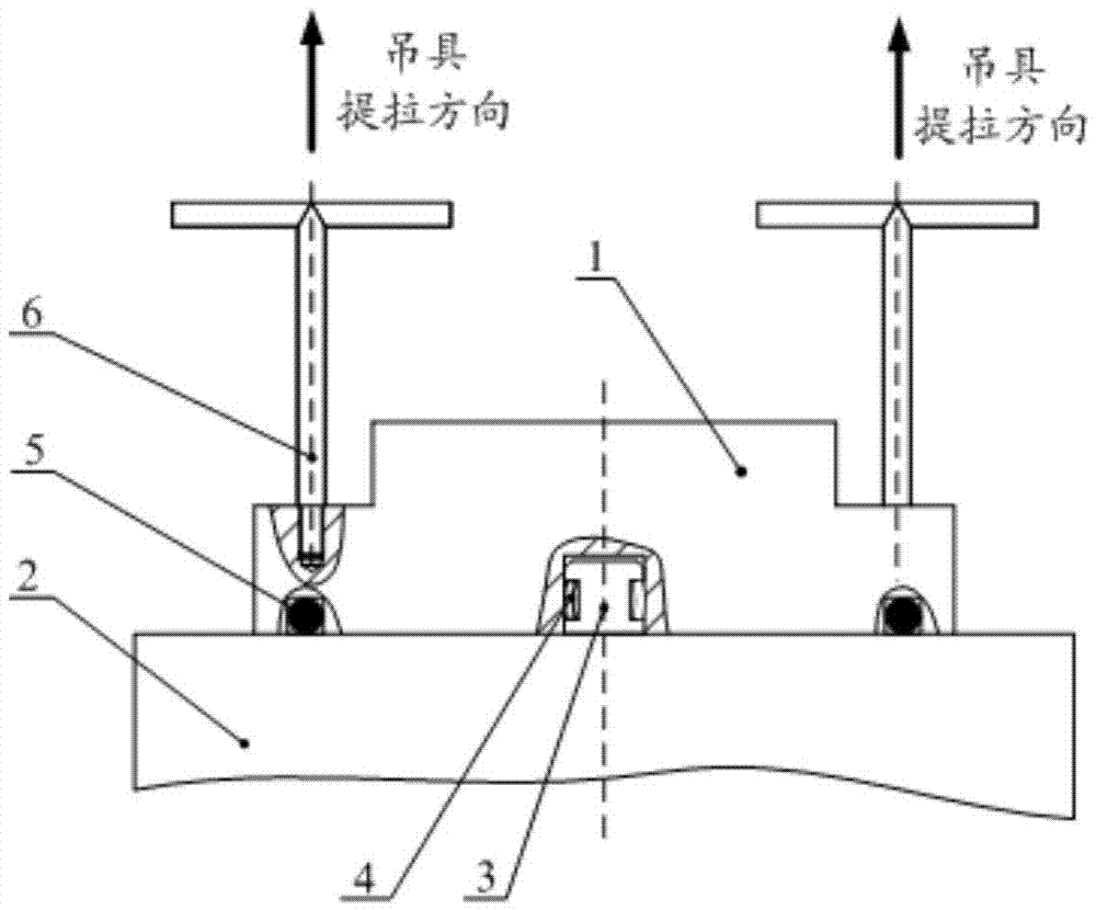
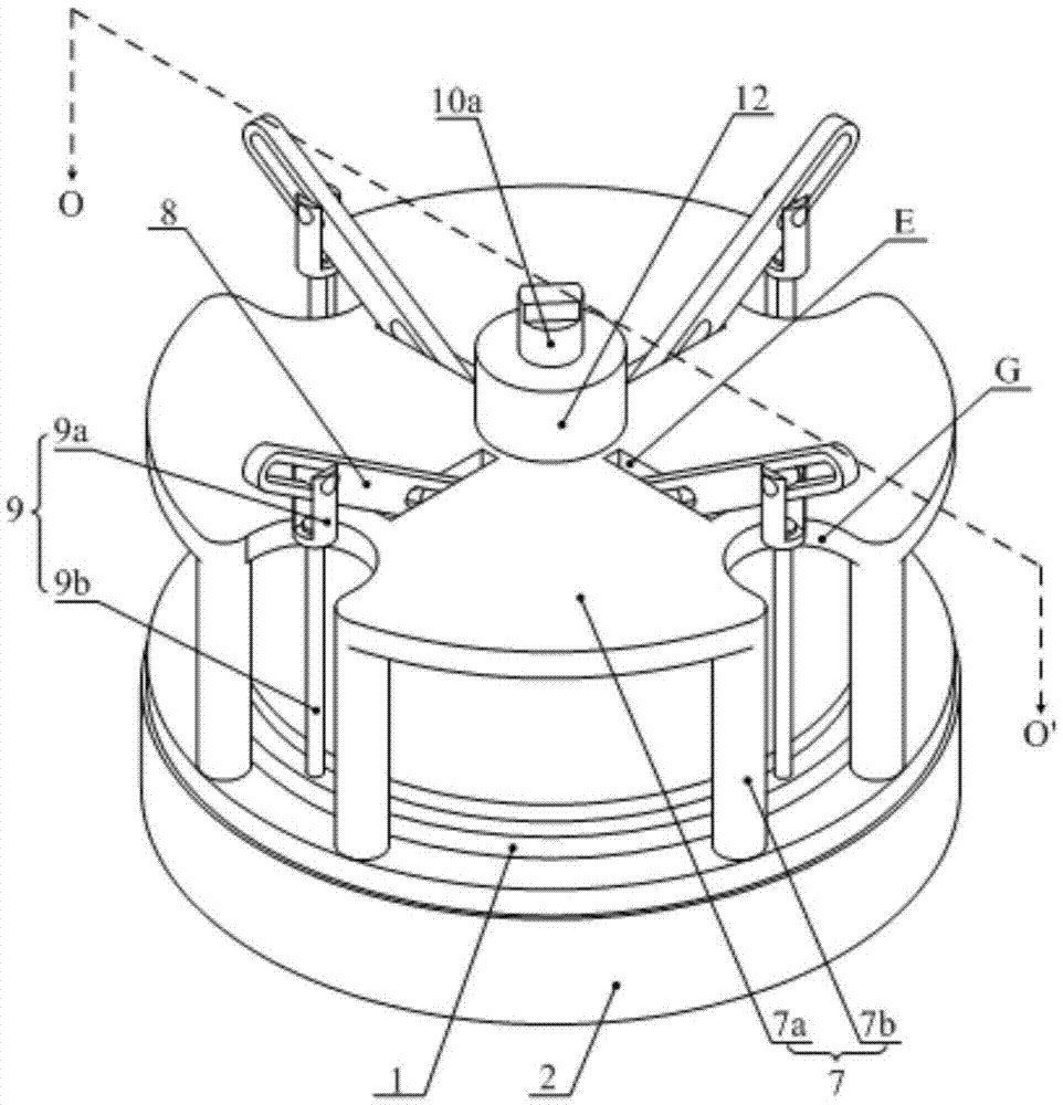
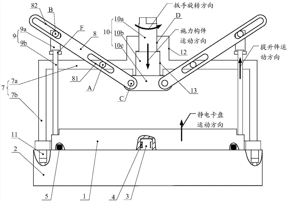
[0033] This embodiment provides a device for removing an electrostatic chuck, such as Figure 2 to Figure 5 As shown, the device for removing the electrostatic chuck includes multiple sets of lever structures, a force applying member 10 and a base frame 7 . Wherein, each group of lever structures includes a lever 8 and a lifting member 9, and t...
PUM
 Abstract
Description
Claims
Application Information