Spin MOSFET

a technology of spin mosfet and mosfet plate, which is applied in the field of spin mosfet, can solve the problems of reducing affecting the reliability of the devi

Inactive Publication Date: 2009-10-13
KK TOSHIBA
View PDF10 Cites 38 Cited by
  • Summary
  • Abstract
  • Description
  • Claims
  • Application Information

AI Technical Summary

Benefits of technology

[0012]The present invention has been made in view of these circumstances, and an object thereof is to provide a spin MOSFET that performs a spin reversal at a low current density and achieves large output characteristics through the spin reversal.

Problems solved by technology

However, in a case where this spin injecting technique is applied to a spin tunnel device, a problem of a defective device is caused by breakdown of the tunnel insulating film, for example.
This reduces the reliability of the device.

Method used


Image

  • Spin MOSFET
  • Spin MOSFET
  • Spin MOSFET

Examples


first embodiment

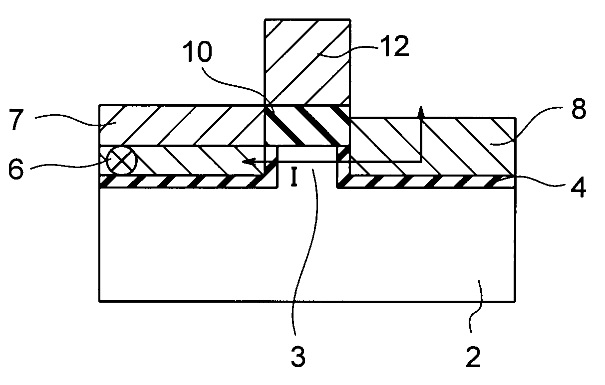
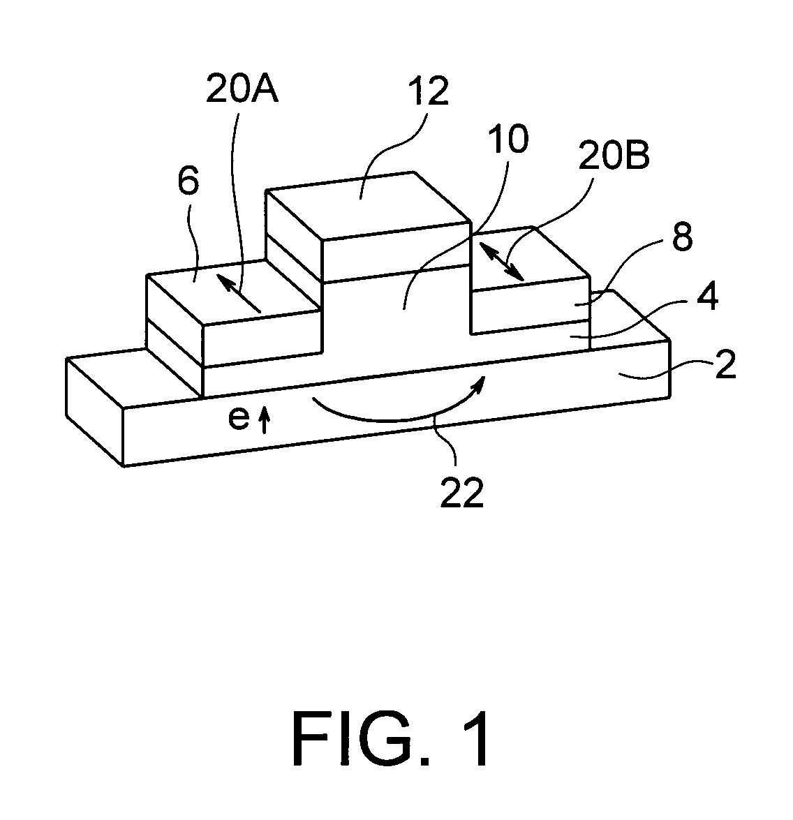
[0086]FIG. 3 is a cross-sectional view of a spin MOSFET in accordance with a first embodiment of the present invention. The spin MOSFET of this embodiment has a semiconductor substrate 2 made of silicon, for example, and a first magnetic film 6 and a second magnetic film 8 arranged at a distance from each other on the semiconductor substrate 2. The first magnetic film 6 in which a magnetization direction is pinned serves as a source or a drain. The second magnetic film 8 in which a magnetization direction is changeable serves as a source or a drain. A tunnel insulating film 4 is formed in the junction plane between the semiconductor substrate 2 and the first and second magnetic films 6 and 8. A gate insulating film 10 is formed on a region 3 (a channel region 3) of the semiconductor substrate 2 between the first and second magnetic films 6 and 8. A gate electrode 12 is formed on the gate insulating film 10. An antiferromagnetic layer 7 that pins the magnetization direction of the fi...

second embodiment

[0110]FIG. 6 is a cross-sectional view of a spin MOSFET in accordance with a second embodiment of the present invention.

[0111]The spin MOSFET of this embodiment is the same as the spin MOSFET of the first embodiment shown in FIG. 3, except that the antiferromagnetic layer 7 is removed, and the first magnetic film 6 as a single-layer ferromagnetic layer is replaced with a first magnetic film 6A that has a stacked structure formed with a synthetic magnetization pinned layer and an antiferromagnetic layer 6a. As shown in FIG. 7A, the magnetization pinned layer has a stacked structure formed with a ferromagnetic layer 61, a nonmagnetic layer 62, and a ferromagnetic layer 63, and the antiferromagnetic layer 6a pins the magnetization direction of the magnetization pinned layer. The ferromagnetic layer 61 and the ferromagnetic layer 63 are antiferromagnetically coupled to each other via the nonmagnetic layer 62.

[0112]FIG. 7B shows a first specific example of the second magnetic film 8 of t...

third embodiment

[0122]FIG. 9 is a cross-sectional view of a spin MOSFET in accordance with a third embodiment of the present invention. The spin MOSFET of this embodiment is a Schottky spin MOSFET, and is the same as the spin MOSFET of the first embodiment shown in FIG. 3, except that the tunnel insulating film 4 is removed from the structure.

[0123]Accordingly, a specific example structure of the second magnetic film 8 of this embodiment has the multilayer structure shown in FIG. 4A or 4B, like the second magnetic film 8 of the first embodiment. In a case where the second magnetic film 8 has the multilayer structure shown in FIG. 4A, the ferromagnetic layer of the first magnetic film 6 and the ferromagnetic layers 81, 83, and 85 of the second magnetic film 8 have the magnetic directions shown in FIG. 5, as in the first embodiment.

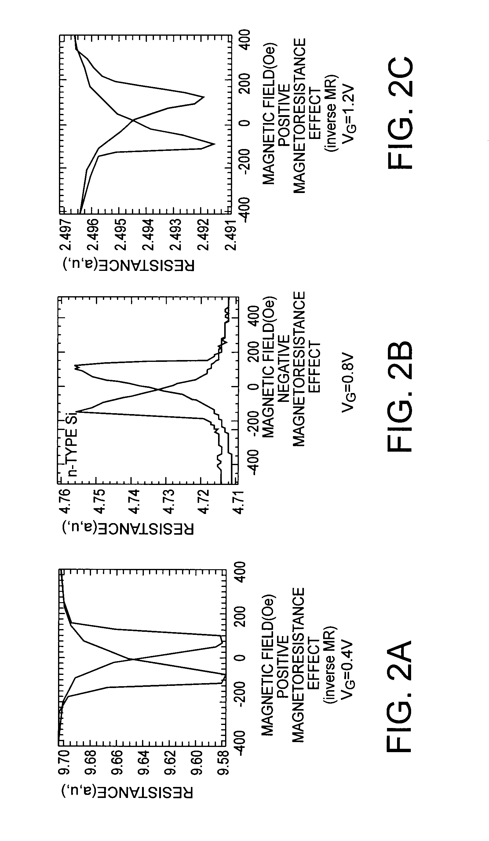
[0124]As in the first embodiment, a gate voltage that causes the negative magnetoresistance effect shown in FIG. 2B is used for writing. In this manner, the inversion curr...


PUM


Abstract

A spin MOSFET includes: a semiconductor substrate; a first magnetic film formed on the semiconductor substrate and including a first ferromagnetic layer, a magnetization direction of the first ferromagnetic layer being pinned; a second magnetic film formed on the semiconductor substrate to separate from the first magnetic film and including a magnetization free layer, a first nonmagnetic layer being a tunnel insulator and provided on the magnetization free layer, and a magnetization pinned layer provided on the first nonmagnetic layer, a magnetization direction of the magnetization free layer being changeable and a magnetization direction of the magnetization pinned layer being fixed; a gate insulating film provided at least on the semiconductor substrate between the first magnetic film and the second magnetic film; and a gate electrode formed on the gate insulating film.

Description

CROSS-REFERENCE TO RELATED APPLICATION[0001]This application is based upon and claims the benefit of priority from prior Japanese Patent Application No. 2006-244656 filed on Sep. 8, 2006 in Japan, the entire contents of which are incorporated herein by reference.BACKGROUND OF THE INVENTION[0002]1. Field of the Invention[0003]The present invention relates to spin MOSFETs.[0004]2. Related Art[0005]In recent years, intensive studies are being made to develop devices such as spin MOSFETs having novel functions. One of those devices is a spin MOSFET that has the source-drain region formed with a magnetic material. Such a spin MOSFET is characterized in that the output characteristics can be controlled simply by reversing the spin moment direction of the magnetic material of the source-drain region. This feature can be utilized to form spin MOSFETs that have amplifying functions as well as reconfigurable functions, and to form a reconfigurable logic circuit with those spin MOSFETs.[0006]T...

Claims


Application Information

Patent Timeline
Patent Type & Authority Patents(United States)
IPC IPC(8): G11C11/00
CPCB82Y25/00H01L29/66984H01F10/3254H01F10/1936H01F10/3272
Inventor SAITO, YOSHIAKISUGIYAMA, HIDEYUKIINOKUCHI, TOMOAKI
Owner KK TOSHIBA
Why Eureka
Try Eureka