A non-damaging dry overetching preparation method of Schottky junction

A technology of Schottky junction and dry etching, which is applied in semiconductor/solid-state device manufacturing, semiconductor/solid-state device testing/measurement, semiconductor devices, etc., can solve the problems of etching damage epitaxial materials and uncontrollable process accuracy, and achieve Precisely Controlled Effects

Active Publication Date: 2020-06-19
INST OF MICROELECTRONICS CHINESE ACAD OF SCI
View PDF3 Cites 0 Cited by
  • Summary
  • Abstract
  • Description
  • Claims
  • Application Information

AI Technical Summary

Problems solved by technology

[0005] In view of the above technical problems, the present invention provides a non-damaging dry overetching preparation method for Schottky junctions, which solves the problem of overetch damage to epitaxial materials in the prior art, and the wet etching process In order to solve the problem that the process precision cannot be controlled, the present invention can produce high-quality Schottky junctions without increasing the cost

Method used


Image

  • A non-damaging dry overetching preparation method of Schottky junction
  • A non-damaging dry overetching preparation method of Schottky junction
  • A non-damaging dry overetching preparation method of Schottky junction

Examples


Embodiment Construction

[0031] In order to make the objectives, technical solutions, and advantages of the present invention clearer, the following further describes the present invention in detail in conjunction with specific embodiments and with reference to the accompanying drawings.

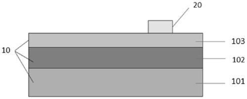
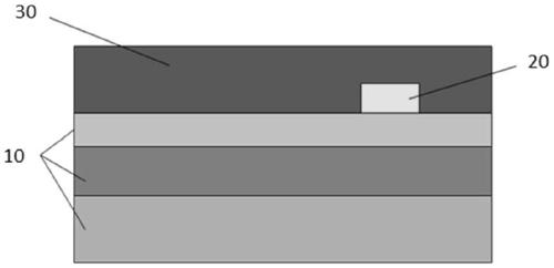
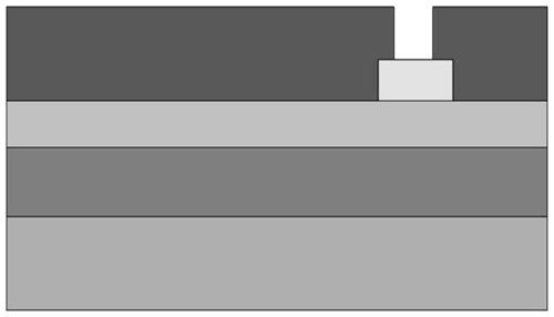
[0032] In an exemplary embodiment of the present invention, a non-destructive dry over-etching preparation method of Schottky junction is provided, which includes the following steps: First, lift is used at the position where the Schottky junction is prepared on the upper surface of the epitaxial wafer. -off method to form a metal barrier layer; then, an insulating dielectric layer is grown on the upper surface of the epitaxial wafer and the upper surface of the metal barrier layer; then, dry etching is used to conduct the insulating medium at the position where the Schottky junction is prepared Etching to form Schottky holes, in which, the scanning electron microscope SEM is used to observe whether over-etching is achi...


PUM

PropertyMeasurementUnit
thicknessaaaaaaaaaa
thicknessaaaaaaaaaa
thicknessaaaaaaaaaa

Abstract

The invention provides a nondestructive dry-method over-etching manufacturing method of a Schottky junction. The method comprises the following steps of S1, forming a metal barrier layer at a position of an upper surface of an epitaxial wafer, wherein the Schottky junction is manufactured at the position; S2, growing insulation dielectric layers on the upper surface of the epitaxial wafer and an upper surface of the metal barrier layer; S3, using a dry etching method to carry out over etching on an insulating dielectric of the upper surface of the metal barrier layer and forming a Schottky hole; and S4, forming second metal layers on upper surfaces of the insulation dielectric layers and at the Schottky hole, and acquiring the Schottky junction and an anode. In the prior art, during a dry etching process, over etching is performed so that an epitaxial material is damaged, and during a wet etching process, technology precision can not be controlled. By using the method of the invention, the above problems are solved; and under the condition that cost is not increased, the Schottky junction with high quality is made.

Description

Technical field [0001] The present invention relates to the field of semiconductor processing technology, and in particular to a non-damaged dry over-etching preparation method of Schottky junctions. The method can be used to achieve complete non-damage to the epitaxial structure during the entire process of preparing Schottky junctions and is simple and easy. Row. Background technique [0002] Schottky diode is a device similar to PN junction rectification characteristics formed by the contact of metal and lightly doped semiconductor. The Schottky diode is a multi-sub device, so its reverse recovery time is particularly short, and it is especially suitable for higher frequency circuit applications. Schottky diodes are particularly widely used in terahertz circuit applications. However, in order to reduce the junction capacitance of the diode itself and increase its cut-off frequency, the Schottky junction is usually required to be extremely small. For example, the typical appli...

Claims


Application Information

Patent Timeline
Patent Type & Authority Patents(China)
IPC IPC(8): H01L21/329H01L21/311H01L21/66
CPCH01L21/31116H01L22/12H01L29/66143
Inventor 郭栋刘晓宇周静涛杨成樾金智
Owner INST OF MICROELECTRONICS CHINESE ACAD OF SCI
Why Eureka
Try Eureka