OLED pixel structure, OLED substrate and OLED module
A pixel structure and substrate technology, applied in the OLED field, can solve problems such as pixel erosion, damage to organic materials, and device failure, and achieve the effects of preventing pixel shrinkage, water vapor erosion, and device failure
- Summary
- Abstract
- Description
- Claims
- Application Information
AI Technical Summary
Problems solved by technology
Method used
Image
Examples
Embodiment 1
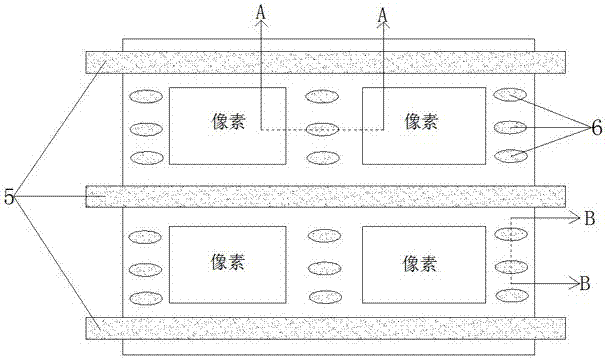
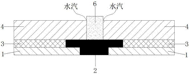
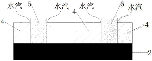
[0027] Such as Figure 1-3 As shown, an OLED pixel structure includes a transparent anode 1, an isolation layer 2 that isolates a matrix pixel area on the transparent anode 1, an organic material 3 in the pixel area, and an isolation layer 2 on the isolation layer 2. Several strip-shaped barrier walls 5 of the metal cathode 4 and several block-shaped barrier walls 6 running perpendicular to the strip-shaped barrier walls 5 , and the metal cathode 4 on the organic material 3 and the isolation layer 2 .
[0028] In the prior art, the matrix pixel structure of the OLED adds several block-shaped barrier ribs 6 that are perpendicular to the strip-shaped barrier walls 5 that isolate the metal cathode 4, that is, several block-shaped barrier ribs are added in the SEGMENT direction of the OLED pixel structure. The wall 6 is equivalent to adding a water vapor release channel in the SEGMENT direction of the OLED pixel structure, which can release the water vapor in the isolation layer 2...
Embodiment 2
[0036] Such as Figure 4 with 5 As shown, an OLED pixel structure includes a transparent anode 1, an isolation layer 2 that isolates a special-shaped pixel area on the transparent anode 1, an organic material 3 in the pixel area, and surrounds the isolated area on the isolation layer 2. Several bulk barrier walls 6 of the organic material 3, the metal cathode 4 on the organic material 3 and the isolation layer 2.
[0037] The odd-shaped pixel structure of the OLED is provided with several block-shaped barrier walls 6 surrounding the organic material 3 on the isolation layer 2, which can release the water vapor in the isolation layer 2 from the several block-shaped barrier walls 6 and be absorbed. The desiccant 11 absorbs and prevents the moisture in the isolation layer 2 from corroding the organic material 3 in the pixel.
[0038]Before the high temperature reliability test of the existing OLED pixel structure without block barrier ribs 6, the OLED pixel structure shrinks by...
Embodiment 3
[0046] Such as Image 6 As shown, an OLED substrate includes a carrier substrate 7 and an OLED device 8 disposed on the carrier substrate 7, and the OLED device 8 includes several OLED pixel structures described in Embodiment 1 or Embodiment 2.
[0047] The carrier substrate 7 is a glass substrate, or a plastic substrate, or a metal substrate, or polyimide, or acrylic.
PUM
 Abstract
Description
Claims
Application Information


