Semiconductor manufacturing device and method

A technology for manufacturing equipment and semiconductors, applied in semiconductor/solid-state device manufacturing, cleaning methods and appliances, chemical instruments and methods, etc., can solve problems such as low-k dielectric damage, improve electrical characteristics and electromagnetic (EM) characteristics, eliminate Damage and the effect of reducing the introduction of impurities

Inactive Publication Date: 2017-08-08
SEMICON MFG INT (SHANGHAI) CORP +1
View PDF4 Cites 2 Cited by
  • Summary
  • Abstract
  • Description
  • Claims
  • Application Information

AI Technical Summary

Problems solved by technology

However, since APC utilizes plasma for pre-cleaning, this can cause damage to the low-k dielectric

Method used


Image

  • Semiconductor manufacturing device and method
  • Semiconductor manufacturing device and method
  • Semiconductor manufacturing device and method

Examples


Embodiment Construction

[0036] Embodiments of the present invention will be described below with reference to the accompanying drawings.

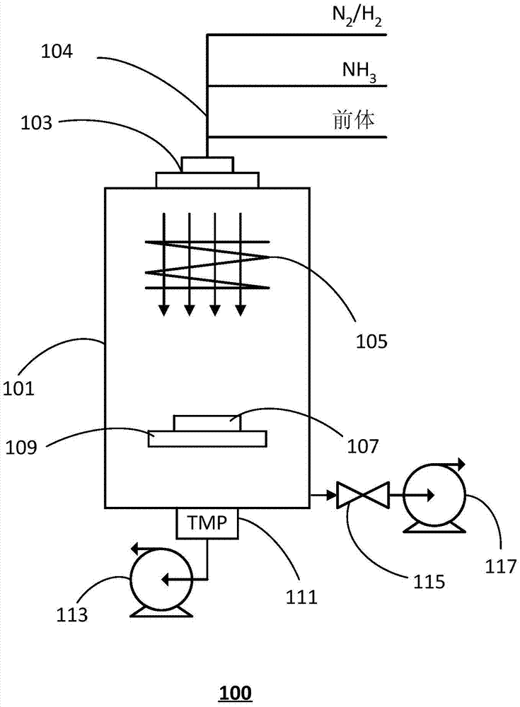
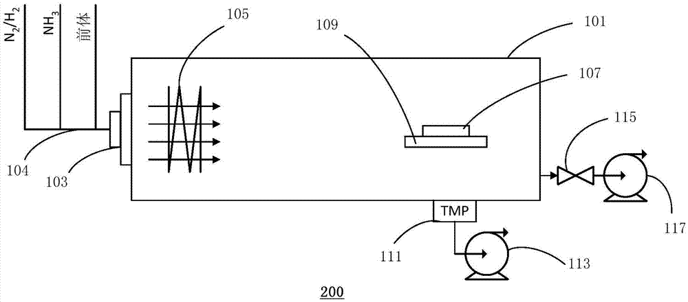
[0037] figure 1 is a schematic diagram showing a semiconductor manufacturing apparatus 100 according to an embodiment of the present invention. Such as figure 1 As shown, a semiconductor fabrication facility 100 according to one embodiment of the present invention includes a cavity housing 101 forming a closed cavity. A substrate to be processed 107 is disposed in the cavity.

[0038] The device 100 also includes a shower head 103, which is arranged on the casing 101, and is used for supplying gas from the outside of the casing to the cavity. In some implementations, the gas can include a process gas. In other implementation manners, the gas may include process gas, carrier gas, and the like. Preferably, the temperature of the gas is 80 to 110 degrees Celsius, for example 100 degrees Celsius. Depending on the application of the device, the process gas may in...


PUM


Abstract

The invention relates to a semiconductor manufacturing device and method. The semiconductor manufacturing device comprises a casing, a spray head and a hot wire; an enclosed chamber is formed in the casing, and a substrate to be processed is arranged in the chamber; the spray head is arranged on the casing, and used to supply gas including a process gas from the outside of the casing to the internal of the chamber; and the hot wire is arranged between the spray head and the substrate to be processed, and is heated during work, gas from the spray head flows through the hot wire, the hot wire ionizes the process gas, and ionized gas is provided for the substrate to be processed. The device may further comprises a hot plate which is arranged in the chamber, supports the substrate to be processed, and heats the substrate to be processed.

Description

technical field [0001] The invention relates to the technical field of semiconductors, in particular to semiconductor manufacturing equipment and manufacturing methods. Background technique [0002] As semiconductor manufacturing process nodes continue to shrink, nucleation layers with lower resistance and better adhesion are required. On the other hand, due to its relatively poor step coverage, physical vapor deposition (PVD) needs to be replaced by atomic layer deposition (ALD) to form a good conformal deposition as the critical dimension decreases. [0003] Although ALD has almost 100% step coverage, it is difficult to avoid impurities such as halogens, oxygen, and carbon, etc. in the deposited film. These impurities will degrade the electrical and electromagnetic (EM) properties of the film and the device. [0004] In conventional current-node manufacturing processes, advanced pre-clean (Advance pre-clean, APC) technology has been used to remove residual polymer and me...

Claims


Application Information

Patent Timeline
Patent Type & Authority Applications(China)
IPC IPC(8): H01L21/67H01L21/02H01L21/318H01L21/3205
CPCH01L21/02057H01L21/02183H01L21/022H01L21/0228H01L21/32051H01L21/67011C23C16/0227C23C16/18C23C16/34C23C16/452C23C16/45544H01L21/02063H01L21/28562H01L21/76814H01L21/76843H01L21/76876B08B7/0035C23C16/45536H01L21/76846H01L21/76879
Inventor 袁光杰周俊卿张海洋
Owner SEMICON MFG INT (SHANGHAI) CORP
Why Eureka
Try Eureka