High-resistance carbon film circuit board and manufacturing method therefor

A manufacturing method and high-resistance technology, applied in printed circuit manufacturing, printed circuit, printed circuit, etc., can solve problems such as high defect rate, failure to apply products, and affect product performance, so as to reduce resistance change rate, uniform carbon distribution, Effect of reducing film thickness

Pending Publication Date: 2017-08-08
东莞福哥电子有限公司
View PDF5 Cites 5 Cited by
  • Summary
  • Abstract
  • Description
  • Claims
  • Application Information

AI Technical Summary

Problems solved by technology

[0002] With the rapid development of science and technology, carbon film printed circuit boards are often used in electrical appliances and instruments, which tend to be multi-functional and miniaturized, and are gradually adopted. They are used in many fields, such as machine tools, automotive control components, and home appliances. Products, electronic toys, etc., when printing carbon film on the surface of printed circuit boards in electronic products, the electrical impedance value is generally in the range of 1kΩ-500kΩ, which cannot be applied to products with high voltage input, so the carbon film with high resistance is specially developed printed circuit board
[0003] The existing high-resistance carbon film circuit boards are realized through traditional screen printing technology. A layer of high-resistance carbon ink is directly printed on the conductive metal layer with a screen with a thickness of more than 30 μm, and the thickness of the formed high-resistance carbon film is The high-resistance carbon ink mainly includes resin and carbon. Due to the large film thickness, the carbon distribution is uneven, and the resistance value of different positions of the high-resistance carbon film varies greatly, that is, the resistance value of the formed product has a large change rate. The high defect rate leads to the instability of the formed product and affects the performance of the product

Method used


Image

  • High-resistance carbon film circuit board and manufacturing method therefor

Examples


Embodiment Construction

[0022] In order to further understand the features, technical means, and specific objectives and functions achieved by the present invention, the present invention will be further described in detail below in conjunction with the accompanying drawings and specific embodiments.

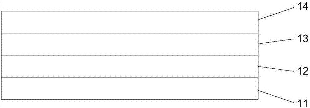
[0023] refer to figure 1 .

[0024] The embodiment of the present invention discloses a method for manufacturing a high-resistance carbon film circuit board, including the following steps:

[0025] a. Design the screen pattern, and make the screen, and set the thickness of the screen to 18-22 μm;

[0026] b. Lay the silk screen on the PCB board 11, print the conductive metal paste on the PCB board 11 through the screen with a squeegee, and form the conductive metal circuit 12 after drying;

[0027] c. Lay the screen on the conductive metal circuit 12, print the high-resistance ink on the conductive metal circuit 12 with a squeegee, and form the first high-resistance carbon film 13 after drying, the t...


PUM


Abstract

The invention provides a manufacturing method for a high-resistance carbon film circuit board. The manufacturing method comprises the following steps of a, designing a silk screen pattern and manufacturing a silk screen; b, printing conductive metal paste on a PCB through silk screen printing by means of frictioning, and performing drying to form a conductive metal circuit; c, printing high-resistance ink on the conductive metal circuit through silk screen printing by means of frictioning, and performing drying to form a first high-resistance carbon film, wherein the first high-resistance carbon film is 7-9[mu]m in thickness; and d, paving the silk screen on the first high-resistance carbon film, printing the high-resistance ink on the first high-resistance carbon film through silk screen printing by means of frictioning, and performing drying to form a second high-resistance carbon film, wherein the second high-resistance carbon film is 7-9[mu]m in thickness. According to the manufacturing method, the original one-time printing and shaping process is divided into two times of printing, so that carbon distribution can be more uniform and resistance change rate of the formed product can be lowered; and the high-resistance carbon film is high in stability, so that the yield of the product can be effectively improved.

Description

technical field [0001] The invention relates to the field of printed circuit boards, and specifically discloses a high-resistance carbon film circuit board and a manufacturing method thereof. Background technique [0002] With the rapid development of science and technology, carbon film printed circuit boards are often used in electrical appliances and instruments, which tend to be multi-functional and miniaturized, and are gradually adopted. They are used in many fields, such as machine tools, automotive control components, and home appliances. Products, electronic toys, etc., when printing carbon film on the surface of printed circuit boards in electronic products, the electrical impedance value is generally in the range of 1kΩ-500kΩ, which cannot be applied to products with high voltage input, so the carbon film with high resistance is specially developed printed circuit board. [0003] The existing high-resistance carbon film circuit boards are realized through traditio...

Claims


Application Information

Patent Timeline
Patent Type & Authority Applications(China)
IPC IPC(8): H05K1/11H05K3/12
CPCH05K1/11H05K3/1216H05K2201/09672H05K2203/0502
Inventor 郑伟延
Owner 东莞福哥电子有限公司
Why Eureka
Try Eureka