Via hole chamfer prediction method

A prediction method and via technology, which is applied in the direction of semiconductor/solid-state device testing/measurement, electrical components, circuits, etc., can solve the problems of long time consumption and high cost, and achieve the effect of short time consumption, low cost and simple judgment

Inactive Publication Date: 2017-08-18
CHENGDU BOE OPTOELECTRONICS TECH CO LTD +1
View PDF3 Cites 0 Cited by
  • Summary
  • Abstract
  • Description
  • Claims
  • Application Information

AI Technical Summary

Problems solved by technology

[0005] In order to solve the problem of long time consumption and high cost when using a scanning electron microscope to detect via holes, the embodiment of the present invention provides a method for predicting via hole chamfering

Method used


Image

  • Via hole chamfer prediction method
  • Via hole chamfer prediction method
  • Via hole chamfer prediction method

Examples


Embodiment Construction

[0025] In order to make the purpose, technical solutions and advantages of the present invention clearer, the following will further describe in detail the embodiments of the present invention in conjunction with the accompanying drawings.

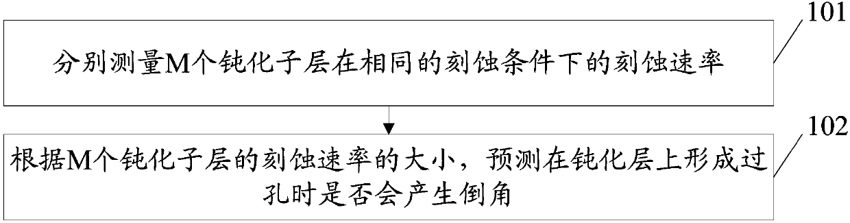
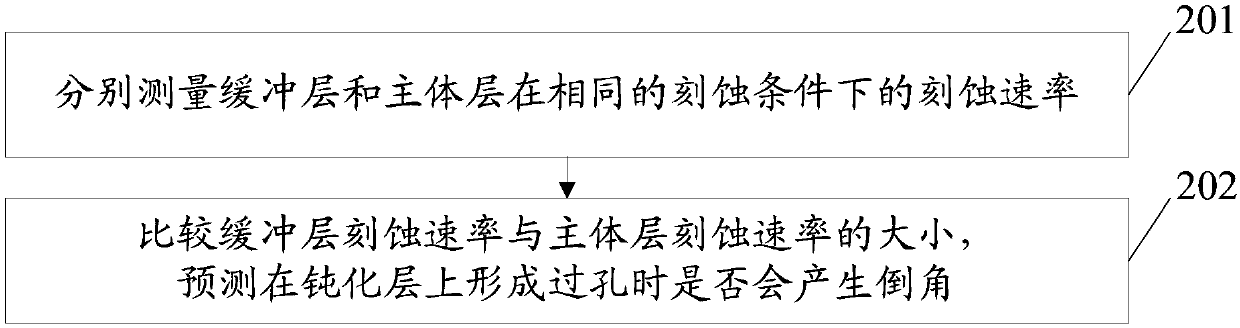
[0026] figure 1 It is a flow chart of a via hole chamfer prediction method provided by an embodiment of the present invention, see figure 1 , the method includes:

[0027] Step 101: Measure the etching rates of M passivation sub-layers under the same etching conditions, M>1, and M is a positive integer.

[0028] In the embodiment of the present invention, the etching rate measurement method of each passivation sub-layer in the M passivation sub-layers is the same, and measuring the etching rate of each passivation sub-layer may include: forming a passivation sub-layer on the substrate layer, and measure the initial film thickness of the passivation sub-layer; etch the passivation sub-layer, and measure the final film thickness of the pas...


PUM

PropertyMeasurementUnit
Thicknessaaaaaaaaaa

Abstract

The invention discloses a via hole chamfer prediction method and belongs to a field of displays. The method includes measuring etching rates of M passivation sublayers in the same etching condition; according to the magnitude of the etching rates to the M passivation sublayers, predicating whether chamfers would be generated or not when via holes are formed in the passivation layer, wherein the passivation layer includes N sublayers arranged in a laminating manner; M sublayers among the N sublayers are corresponding to the passivation sublayers in a one-to-one manner; the sublayers in corresponding arrangement has identical growth condition with the passivation sublayers; M is smaller than or equal to N and is greater than 1 and M, N are both positive integers; the passivation sublayer corresponding to one sublayer which is the lower one in two adjacent sublayers in the M sublayers is the first passivation sublayer and the passivation sublayer corresponding to the other sublayer which is the higher one is the second passivation sublayer. Through measuring and then comparing the etching rates of the at least two passivation sublayers, whether the chamfers would be generated when the via holes are etched in the passivation layers can be predicated. The method is simple in judgment, low in time cost and is also low in cost.

Description

technical field [0001] The invention relates to the field of displays, in particular to a method for predicting chamfering of via holes. Background technique [0002] Thin Film Transistor-Liquid Crystal Display (TFT-LCD) uses the change of the electric field intensity on the liquid crystal molecular layer sandwiched between the upper and lower substrates to change the orientation of the liquid crystal molecules, thereby controlling the intensity of light transmission. A display device to display images. The structure of a liquid crystal display generally includes a backlight module, a polarizer, an array substrate, a color filter (Color Filter, CF) substrate, and a layer of liquid crystal molecules filled in a cell formed by the two substrates. [0003] The array substrate includes a substrate, a gate electrode, a gate insulating layer, an active layer, a source drain electrode and a passivation layer stacked in sequence on the substrate, a pixel electrode is arranged on th...

Claims


Application Information

Patent Timeline
IPC IPC(8): H01L21/66
CPCH01L22/12H01L22/26
Inventor 李惠王丹名李扬黄斗冬
Owner CHENGDU BOE OPTOELECTRONICS TECH CO LTD
Why Eureka
Try Eureka