Multi-input high-speed CMOS buffer circuit

A multi-input and buffer technology, applied in the direction of logic circuit, logic circuit connection/interface layout, logic circuit coupling/interface using field effect transistors, etc., can solve the problem of large circuit power consumption, slow buffer processing speed, increased Buffer complexity and other issues, to achieve the effect of small delay, strong application advantages, and improved ease of use

Active Publication Date: 2017-08-18
SHANGHAI INTEGRATED CIRCUIT RES & DEV CENT +1
View PDF3 Cites 0 Cited by
  • Summary
  • Abstract
  • Description
  • Claims
  • Application Information

AI Technical Summary

Problems solved by technology

This kind of buffer circuit has the following defects: (1) due to the certain impedance and capacitive reactance of the switches, the more switches will cause a larger time delay, which will slow down the processing speed of the buffer; speed, it is usually necessary to increase the bias current of each branch of the circuit, which will lead to a large power consumption of the circuit, (3) when the input signal is too large, a bootstrap switch is required, which increases the complexity of the use of the buffer

Method used


Image

  • Multi-input high-speed CMOS buffer circuit
  • Multi-input high-speed CMOS buffer circuit
  • Multi-input high-speed CMOS buffer circuit

Examples


Embodiment Construction

[0017] In order to make the purpose, technical solution and advantages of the present invention clearer, the specific implementation manners of the present invention will be further described in detail below in conjunction with the accompanying drawings.

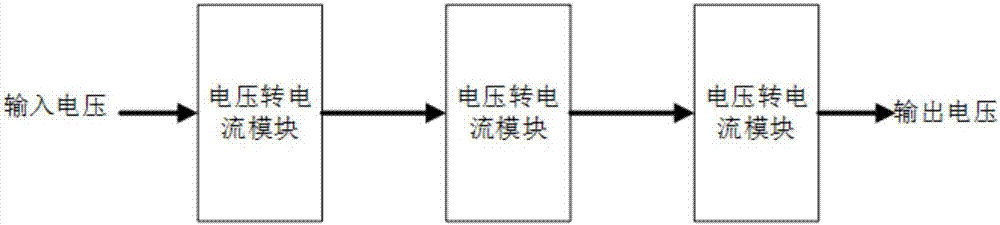
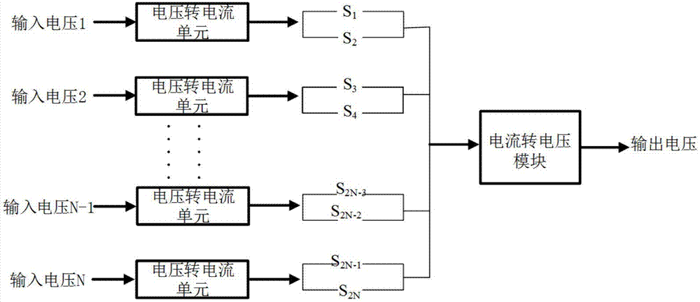
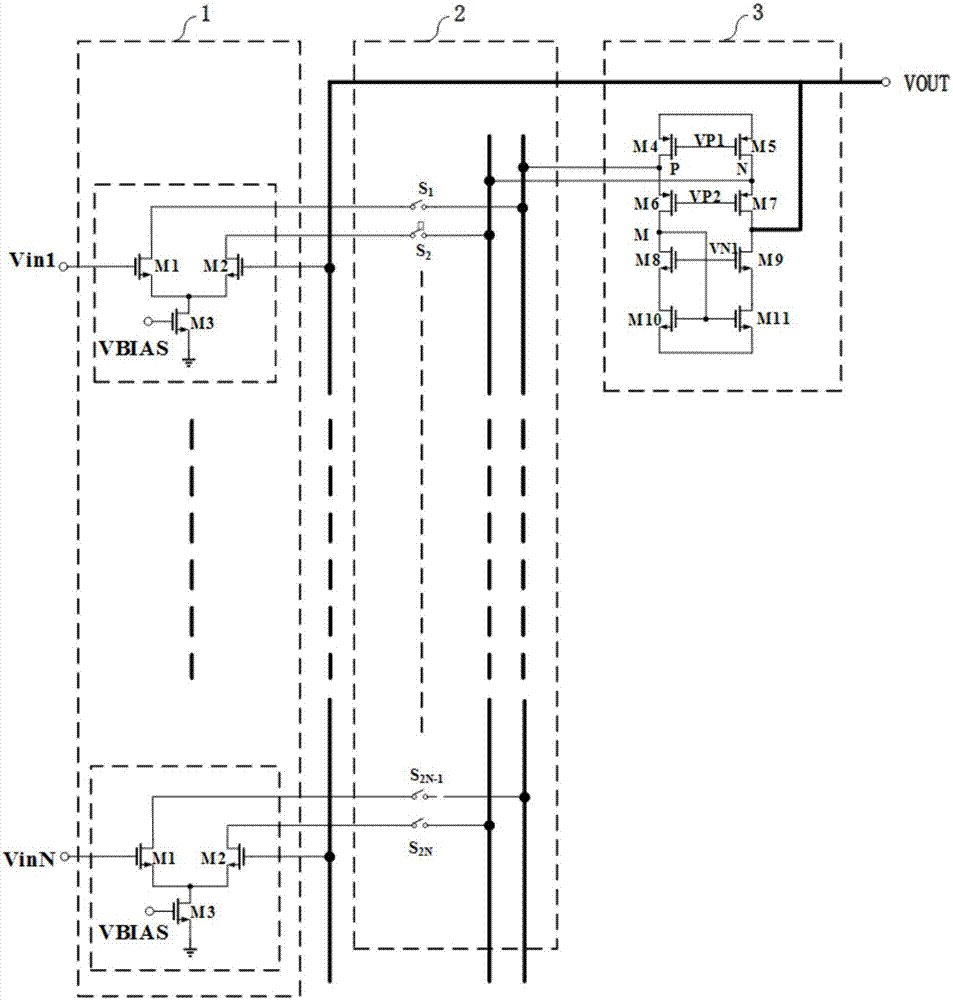
[0018] Such as figure 1 As shown, a multi-input high-speed CMOS buffer circuit, which includes a voltage-to-current module, a multiplexer module, and a current-to-voltage module, and the two sides of the multiplexer module are respectively connected to the voltage-to-current module and the current The other side of the voltage-to-voltage module is used for input voltage, and the other side of the current-to-voltage module is used to output voltage; the voltage-to-current module is used to convert multiple input voltages into current signals; multi-way selection The passer module is used to conduct the voltage-to-current module and the current-to-voltage module; the current-to-voltage module converts the input current signal ...


PUM


Abstract

The invention discloses a multi-input high-speed CMOS buffer circuit. The buffer circuit comprises a voltage-to-current module, a multipath selector module, and a current-to-voltage module, wherein two sides of the multipath selector module are respectively connected with the voltage-to-current module and the current-to-voltage module, the other side of the voltage-to-current module is used for inputting the voltage, and the other side of the current-to-voltage module is used for outputting the voltage; the voltage-to-current module is used for converting multiple input voltage into a current signal; the multipath selector module is used for conducting the voltage-to-current module and the current-to-voltage module; the current-to-voltage module is used for converting the input current signal into a voltage signal and outputting the voltage signal. The multi-input high-speed CMOS buffer circuit disclosed by the invention has the excellent characteristics of being fast in buffering speed, small in delay, free from using a bootstrapping switch, and strong in usability.

Description

technical field [0001] The invention relates to a buffer circuit, in particular to a multi-input high-speed CMOS buffer circuit. Background technique [0002] In modern CMOS analog circuits, the buffer circuit is a very commonly used circuit. The buffer has the characteristics of high input impedance, low output impedance, and high driving capability, and is widely used in various ADCs, DACs, and various SOC chips. At present, the industry has higher and higher requirements for buffers in terms of high speed, low power consumption, and low noise. [0003] In a traditional buffer application environment with multiple input signals, the input voltages of multiple input signals are generally selected and connected to the buffer through multiple switches, and then directly output in the form of voltage. This kind of buffer circuit has the following defects: (1) due to the certain impedance and capacitive reactance of the switches, the more switches will cause a larger time del...

Claims


Application Information

Patent Timeline
Patent Type & Authority Applications(China)
IPC IPC(8): H03K19/0185H03K17/693
CPCH03K17/693H03K19/018521
Inventor 段杰斌袁庆何学红皮常明温建新
Owner SHANGHAI INTEGRATED CIRCUIT RES & DEV CENT
Why Eureka
Try Eureka