Tandem organic photovoltaic devices that include a metallic nanostructure recombination layer
A technology of organic photovoltaic devices and metal nanostructures, which is applied in photovoltaic power generation, electric solid-state devices, semiconductor devices, etc., and can solve problems such as reducing short-circuit current density
- Summary
- Abstract
- Description
- Claims
- Application Information
AI Technical Summary
Problems solved by technology
Method used
Image
Examples
Embodiment Construction
[0022] The organic photovoltaic device and its forming method are described in various embodiments herein. It should be understood that variations in each of these embodiments and other embodiments that are not specifically described in order to clarify and / or avoid the length of the disclosure are possible. In addition, the order, amplitude, and composition of the various layers and structures disclosed herein can be changed, changed, divided or subdivided to meet changing performance requirements.
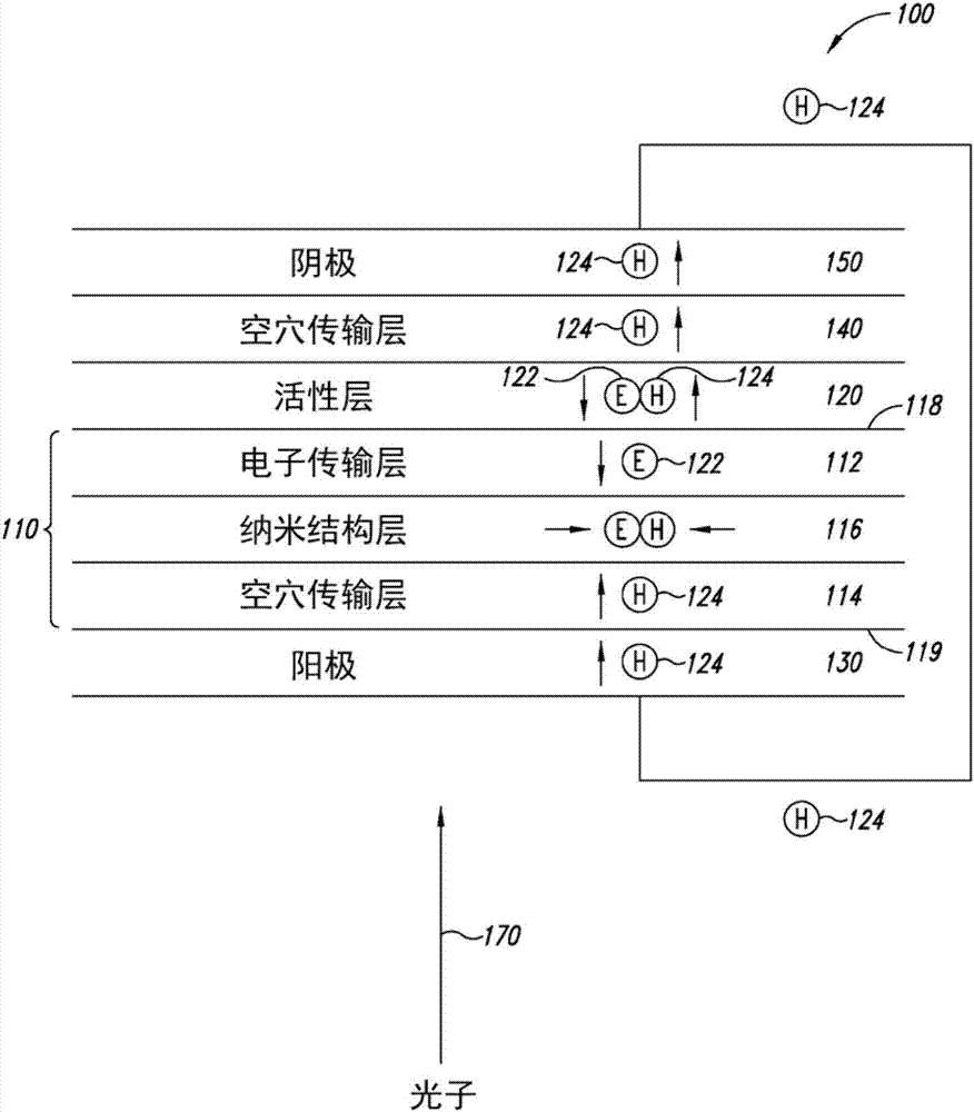
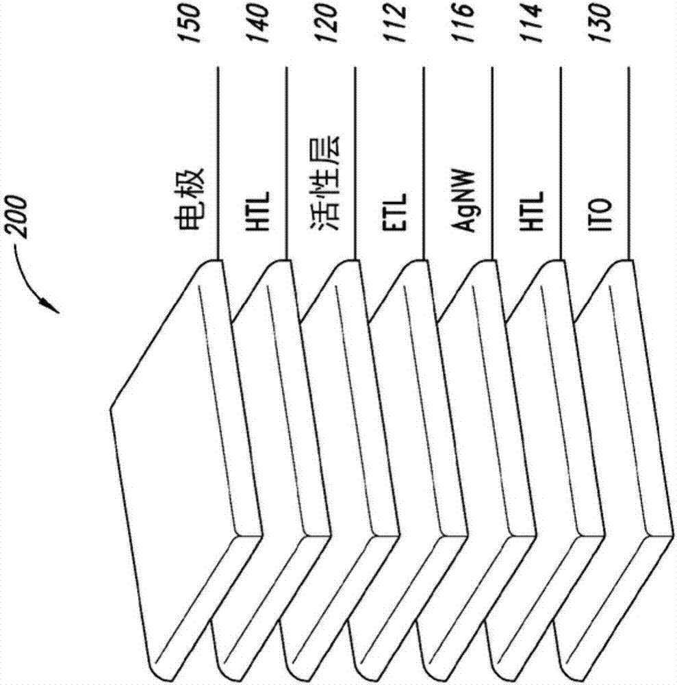
[0023] figure 1 An organic photovoltaic device including an intermediate layer 110 is shown. The intermediate layer 110 includes an electron transport layer 112, a hole transport layer 114, and a metal nanostructure inserted between the active layer 120 and the first electrode 130 of the single junction organic photovoltaic 100 层116. The single junction organic photovoltaic 100 also includes a hole transport layer 140 deposited between the active layer 120 and the second electrode ...
PUM
 Abstract
Description
Claims
Application Information


