OLED (Organic Light Emitting Diode) array substrate, manufacture method thereof and touch display device

A technology of an array substrate and a manufacturing method, which is applied in the display field, can solve the problems of reducing the scope of application of flexible AMOLEDs, integrating touch structures, etc., and achieve the effect of improving the scope of application

Active Publication Date: 2017-08-25
BOE TECH GRP CO LTD +1
View PDF8 Cites 31 Cited by
  • Summary
  • Abstract
  • Description
  • Claims
  • Application Information

AI Technical Summary

Problems solved by technology

However, flexible AMOLED usually adopts ThinFilm Encapsulation (TFE) process. Since the encapsulation film layer used in thin film encapsulation is soft...

Method used


Image

  • OLED (Organic Light Emitting Diode) array substrate, manufacture method thereof and touch display device
  • OLED (Organic Light Emitting Diode) array substrate, manufacture method thereof and touch display device
  • OLED (Organic Light Emitting Diode) array substrate, manufacture method thereof and touch display device

Examples


Embodiment Construction

[0039] The following will clearly and completely describe the technical solutions in the embodiments of the present invention with reference to the accompanying drawings in the embodiments of the present invention. Obviously, the described embodiments are only some of the embodiments of the present invention, not all of them. Based on the embodiments of the present invention, all other embodiments obtained by persons of ordinary skill in the art without making creative efforts belong to the protection scope of the present invention.

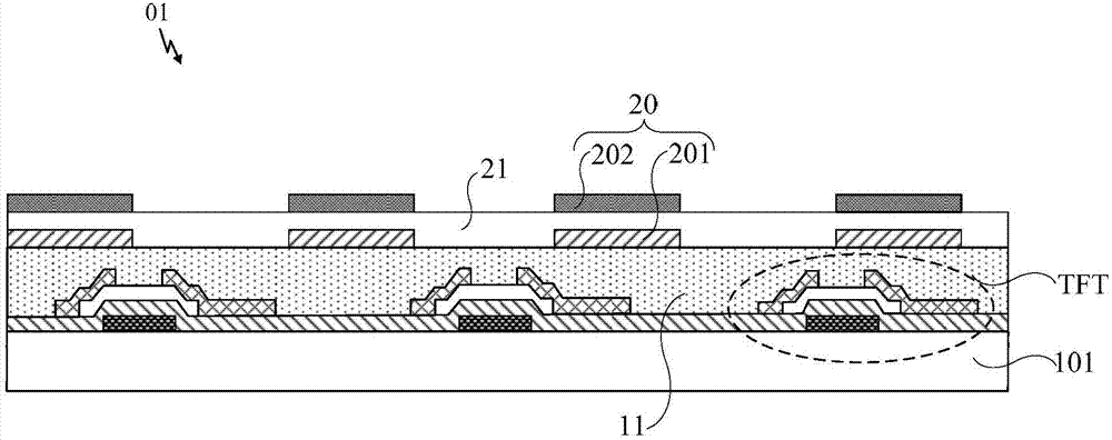
[0040] An embodiment of the present invention provides an OLED array substrate 01, such as figure 1 As shown, it includes a base substrate 101 , a thin film transistor (Thin Film Transistor, TFT) disposed on the base substrate 101 , and a planarization layer 11 covering the thin film transistor (hereinafter referred to as TFT).

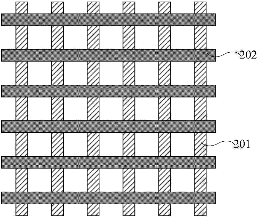
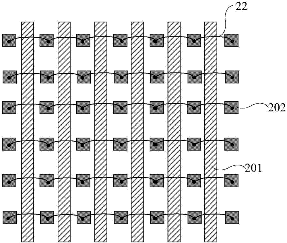
[0041] On this basis, the OLED array substrate 01 further includes a touch sensor 20 located on the side of the planar...


PUM


Abstract

The embodiment of the invention provides an OLED (Organic Light Emitting Diode) array substrate, a manufacture method thereof and a touch display device, relates to the technical field of display, and can integrate a touch structure into a flexible AMOLED (Active Matrix/Organic Light Emitting Diode). The OLED array substrate comprises an underlying substrate, a thin film transistor arranged on the underlying substrate, and a flat layer which covers the thin film transistor. The OLED array substrate also comprises a touch sensor positioned on one side, which deviates from the thin film transistor, of the flat layer, and the touch sensor comprises a first touch electrode and a second touch electrode, wherein the firs touch electrode and the second touch electrode are mutually insulated.

Description

technical field [0001] The present invention relates to the field of display technology, in particular to an OLED array substrate, a manufacturing method thereof, and a touch display device. Background technique [0002] AMOLED (Active Matrix Organic Light Emitting Diode Display, active matrix drive organic light emitting diode display device) has the advantages of low manufacturing cost, high response speed, power saving, DC drive for portable devices, and wide operating temperature range. It is expected to become the next generation of new flat-panel displays to replace LCD (Liquid Crystal Display, Liquid Crystal Display). In particular, flexible AMOLED is attracting more and more attention from the market because of its advantages of being thin and light, bendable or foldable, and capable of changing shape arbitrarily. [0003] For AMOLED, it is usually necessary to set up an encapsulation cover plate to achieve the function of blocking water and oxygen. The above-menti...

Claims


Application Information

Patent Timeline
IPC IPC(8): G06F3/041H01L27/32H01L51/56
CPCG06F3/0412G06F2203/04103H10K59/40H10K71/00G06F3/0446H10K59/122H10K50/84
Inventor 何剑
Owner BOE TECH GRP CO LTD
Why Eureka
Try Eureka