Array substrate, manufacturing method thereof and display device

An array substrate and manufacturing method technology, applied in the display field, can solve the problems of increasing the parasitic capacitance of gate lines and data lines, reducing the aperture ratio of products, etc., and achieve the effects of reducing parasitic capacitance, ensuring aperture ratio, and reducing line resistance

Active Publication Date: 2017-08-25
BOE TECH GRP CO LTD
View PDF7 Cites 7 Cited by
  • Summary
  • Abstract
  • Description
  • Claims
  • Application Information

AI Technical Summary

Problems solved by technology

[0003] However, in the manufacturing process of the array substrate in the prior art, the wider gate lines and data lines tend to reduce the aperture ratio of the product, and increase the parasitic capacitance generated between the gate lines and the data lines

Method used


Image

  • Array substrate, manufacturing method thereof and display device
  • Array substrate, manufacturing method thereof and display device
  • Array substrate, manufacturing method thereof and display device

Examples


Embodiment Construction

[0029] In order for those skilled in the art to better understand the technical solution of the present invention, the array substrate, its manufacturing method, and display device provided by the present invention will be described in detail below with reference to the accompanying drawings.

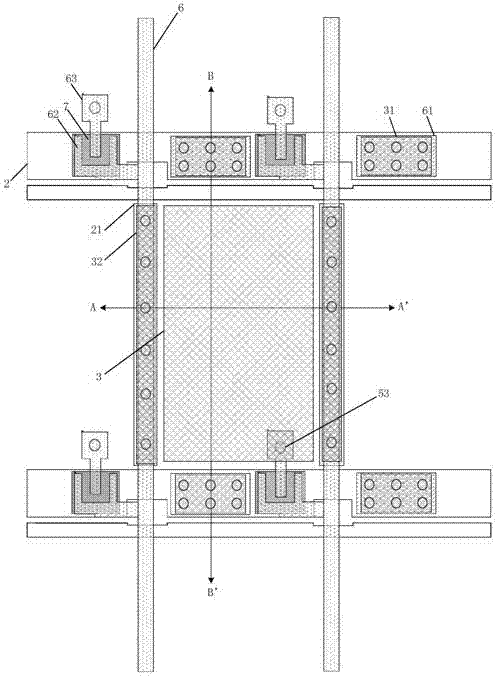
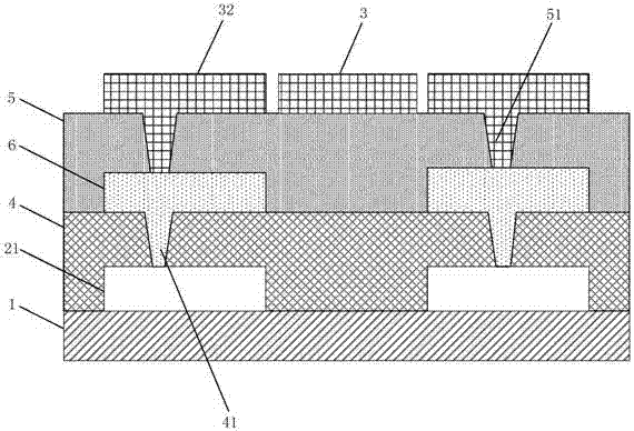
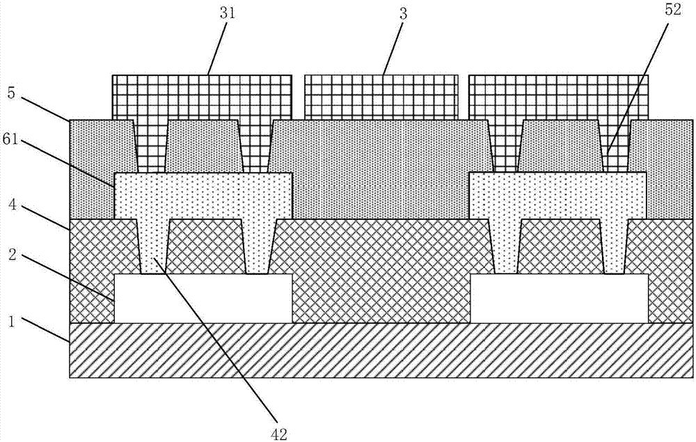
[0030] figure 1 It is a schematic structural diagram of an array substrate provided in Embodiment 1 of the present invention, figure 2 for figure 1 The A-A' cross-sectional view of the array substrate in image 3 for figure 1 The B-B' cross-sectional view of the medium array substrate, such as Figure 1 to Figure 3 As shown, the array substrate includes a base substrate 1, a signal line on the base substrate 1 and at least one connection pattern, and the connection pattern is connected in parallel with the signal line.

[0031] In this embodiment, the signal lines include gate lines or data lines. The number of signal lines is plural. Wherein, preferably, the multiple signal line...


PUM


Abstract

The invention provides an array substrate, a manufacturing method thereof and a display device. The array substrate comprises a substrate base plate, signal lines and at least one connection pattern, and is characterized in that the signal lines and the at least one connection pattern are located on the substrate base plate, and the at least one connection pattern is connected with the signal lines in parallel. According to the array substrate, the manufacturing method thereof and the display device provided by the invention, the at least one connection pattern is connected with the signal lines in parallel, so that line resistance of the signal lines can be reduced without fabricating wide signal lines, the aperture ratio of products is ensured, and parasitic capacitance generated between the signal lines is reduced.

Description

technical field [0001] The present invention relates to the field of display technology, in particular to an array substrate, a manufacturing method thereof, and a display device. Background technique [0002] In the manufacturing process of large-sized array substrates, in order to avoid the low charge rate of the end of the gate lines and data lines due to the excessively long gate lines and data lines, it is usually used to reduce the charging rate by making wider gate lines and data lines. The line resistance of the signal line is small, thereby improving the terminal charging rate of the gate line and the data line. [0003] However, in the manufacturing process of the array substrate in the prior art, wider gate lines and data lines tend to reduce the aperture ratio of the product, and increase the parasitic capacitance generated between the gate lines and the data lines. Contents of the invention [0004] The invention provides an array substrate, its manufacturing...

Claims


Application Information

Patent Timeline
Patent Type & Authority Applications(China)
IPC IPC(8): H01L27/12H01L21/84
CPCH01L27/124H01L27/1259
Inventor 冯京
Owner BOE TECH GRP CO LTD
Why Eureka
Try Eureka