Circuit board for ink jet head, method of manufacturing the same, and ink jet head using the same

a technology of ink jet head and circuit board, which is applied in the direction of printing, etc., can solve the problems that the circuit board cannot be secured without increasing the size of the circuit board, and the heater b, /b> is subject to a severe environment, so as to prevent the increase of the circuit board size, reduce the resistance of wires, and improve the effect of integration

Inactive Publication Date: 2006-02-16
CANON KK
View PDF30 Cites 15 Cited by
  • Summary
  • Abstract
  • Description
  • Claims
  • Application Information

AI Technical Summary

Benefits of technology

[0031] With this invention, the electrode wires are formed of a plurality of layers to reduce wire resistances and prevent a size increase of the circuit board. This construction enables high density integration of the heaters required to achieve a high resolution printing, a high printed image quality and a high speed printing. Since in this construction the effective thickness of the protective layers over the heaters can be reduced, the thermal efficiency can be enhanced and the power consumption reduced.
[0032] With this invention, a small, highly reliable ink jet head having nozzles formed at high density can be provided.

Problems solved by technology

In such an ink jet head circuit board, the heater 102 is subjected to a severe environment, including a temperature rise and fall as large as 1,000° C. in a short period of time and also mechanical impacts caused by cavitations from repeated creation and collapse of bubbles.
However, as the number of heaters or energy generation portions formed on the board becomes very large for the reason described above, a sufficient space to accommodate widened electrode wires cannot be secured without increasing the size of the circuit board.
This prevents the protective layers over the heaters from being formed sufficiently thin or results in an increase in a space or area accommodating the thick portion of the protective layers over the heaters.

Method used


Image

  • Circuit board for ink jet head, method of manufacturing the same, and ink jet head using the same
  • Circuit board for ink jet head, method of manufacturing the same, and ink jet head using the same
  • Circuit board for ink jet head, method of manufacturing the same, and ink jet head using the same

Examples


first embodiment

Superiority of First Embodiment

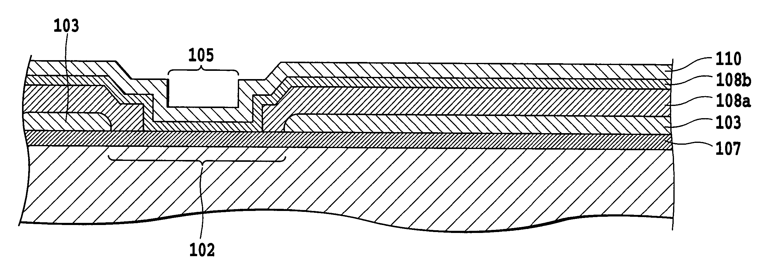
[0064] Fabricating the circuit board in the process described above can not only reduce the resistance of wires and the effective thickness of the protective insulation layer over the heater 102, improve a heat efficiency and reduce an overall power consumption, but also contribute to a higher density of heaters which in turn will realize higher resolution and quality of printed images and a faster printing speed.

[0065] More specifically, the fact that the electrode wires are constructed of a plurality of layers to reduce wire resistance prevents the circuit board from becoming large in size and allows heaters and nozzles to be formed in high density, assuring an improved resolution and quality of printed images and a faster printing speed. In reducing the resistance of electrode wires, a conventional practice involves increasing the width of the electrode wires formed on the circuit board. However, as the number of heaters formed on the board becomes...

second embodiment

of Ink Jet Head Circuit Board and Process of Manufacturing the Same)

[0074]FIG. 15 and FIG. 16 are a schematic plan view showing a heater in the ink jet head circuit board according to the second embodiment of this invention and a schematic cross-sectional view taken along the line XVI-XVI of FIG. 15, respectively. In these figures, components that function in the same way as those of the conventional construction and the first embodiment are given like reference numbers.

[0075] In the construction of this embodiment, the first electrode wire layer 103 and the second electrode wire layer 104 have a thickness relation of t1>t2, where t1 is a thickness of the first electrode wire layer 103 and t2 is a thickness of the second electrode wire layer 104. Next, as stipulated by this invention, after the first protective insulation layer 108 is formed, it is removed from portions 301 above the heater 102.

[0076] Referring to FIG. 17 through FIG. 20, an example process of manufacturing the in...

third embodiment

of Ink Jet Head Circuit Board and Process of Manufacturing the Same

[0086] Although the preceding embodiments employ the two-layer construction for the electrode wires for heater 102, the similar philosophy can be applied where three or more layers are used.

[0087]FIG. 21 and FIG. 22 are a schematic plan view showing a heater in the ink jet head circuit board according to the third embodiment of this invention and a schematic cross-sectional view taken along the line XXII-XXII of FIG. 21, respectively. In these figures, components that function in the same way as those of the conventional construction and the first and second embodiment are given like reference numbers.

[0088] In the construction of this embodiment, the first electrode wire layer 103, the second electrode wire layer 104 and a third electrode wire layer 130 have a thickness relation of t1, t2>t3, where t1, t2 and t3 are the thicknesses of the first, second and third electrode wire layer, respectively. As stipulated by...


PUM


Abstract

An ink jet head circuit board is provided which has heaters to generate thermal energy for ejecting ink as they are energized. This circuit board is so constructed as to reduce wire resistances for the heaters while at the same time preventing an increase in the size of the board and realizing a high-density integration of the heaters required for high resolution printing. This construction is made possible by forming electrode wires of first and second electrode wire layers to reduce an area that the wire patterns for the heater occupy on the circuit board. In reducing the effective thickness of protective insulation layer formed on the heater to prevent a possible degradation of thermal efficiency, one of the protective insulation layers over the electrode wires is removed from the heater, depending on the thickness of the electrode wires.

Description

BACKGROUND OF THE INVENTION [0001] 1. Field of the Invention [0002] The present invention relates to a circuit board for an ink jet head that ejects ink for printing, a method of manufacturing the circuit board, and an ink jet head using the circuit board. [0003] 2. Description of the Related Art [0004] An ink jet printing system has an advantage of low running cost because an ink jet head as a printing means can easily be reduced in size, print a high-resolution image at high speed and even form an image on so-called plain paper that is not given any particular treatment. Other advantages include low noise that is achieved by a non-impact printing system employed by the print head and an ability of the print head to easily perform color printing using multiple color inks. [0005] There are a variety of ejection methods available for the ink jet head to realize the ink jet printing system. Among others, ink jet heads using thermal energy to eject ink, such as those disclosed in U.S. ...

Claims


Application Information

Patent Timeline
Patent Type & Authority Applications(United States)
IPC IPC(8): B41J2/05
CPCB41J2/14072B41J2/1628B41J2/1603B41J2/14129
Inventor ONO, KENJIOZAKI, TERUOSAKAI, TOSHIYASUSAITO, ICHIROIBE, SATOSHIYOKOYAMA, SAKAISHIBATA, KAZUAKI
Owner CANON KK
Why Eureka
Try Eureka