Solar cell and method for producing thereof

a solar cell and cell technology, applied in the field of solar cells, can solve problems such as lowering of fill factor, and achieve the effects of reducing wiring resistance, increasing the number of bus bar electrodes, and shortening the length of finger electrodes

Active Publication Date: 2017-06-15
SHIN ETSU CHEM IND CO LTD
View PDF5 Cites 15 Cited by
  • Summary
  • Abstract
  • Description
  • Claims
  • Application Information

AI Technical Summary

Benefits of technology

[0043]In the inventive solar cell, it is possible to increase the number of the bus bar electrodes, to shorten the length of the finger electrodes, and to collect current from finger electrodes on both sides of the bus bar electrodes by installing insulator films and forming three-dimensional structure of bus bar electrodes and finger electrodes. As a result, it is possible to decrease the wiring resistance and to increase the fill factor. Moreover, it is possible to increase the cross-section of the finger electrode to decrease the wiring resistance while decreasing the contact area by forming the current collectors on the contact portion, and to improve the open-circuit voltage thereby. Furthermore, since the bus bar electrodes are not in contact with the substrate directly, the solar cell will not shunt. Moreover, it is possible to suppress bleeding in forming the bus bar electrodes by flattening the area to form the bus bar electrode, and to improve the yield thereby. Furthermore, the inventive method for producing a solar cell can produce such a solar cell without increasing production steps.

Problems solved by technology

In this arrangement, the finger electrodes are long, and accordingly the wiring resistance becomes extremely large, which causes lowering of a fill factor.

Method used


Image

  • Solar cell and method for producing thereof
  • Solar cell and method for producing thereof
  • Solar cell and method for producing thereof

Examples


examples

[0128]Hereinafter, the present invention will be described in more detail with reference to Example and Comparative Example, but the present invention is not limited this Example.

example 1

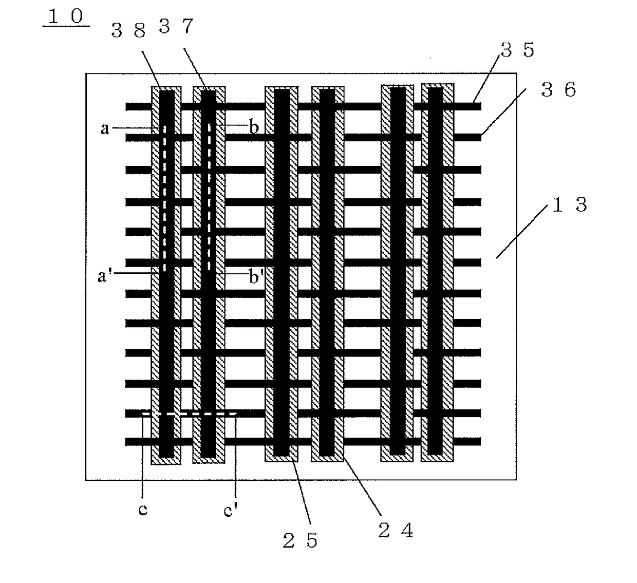
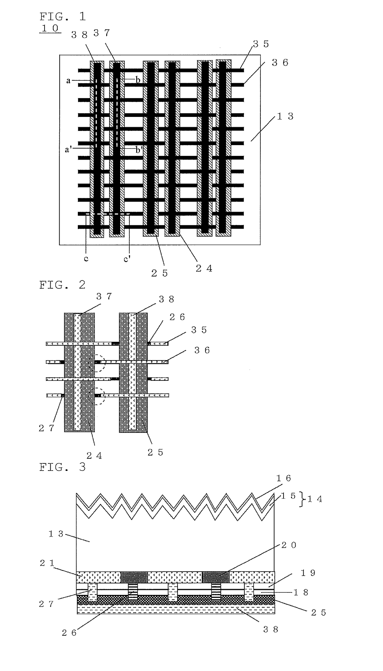
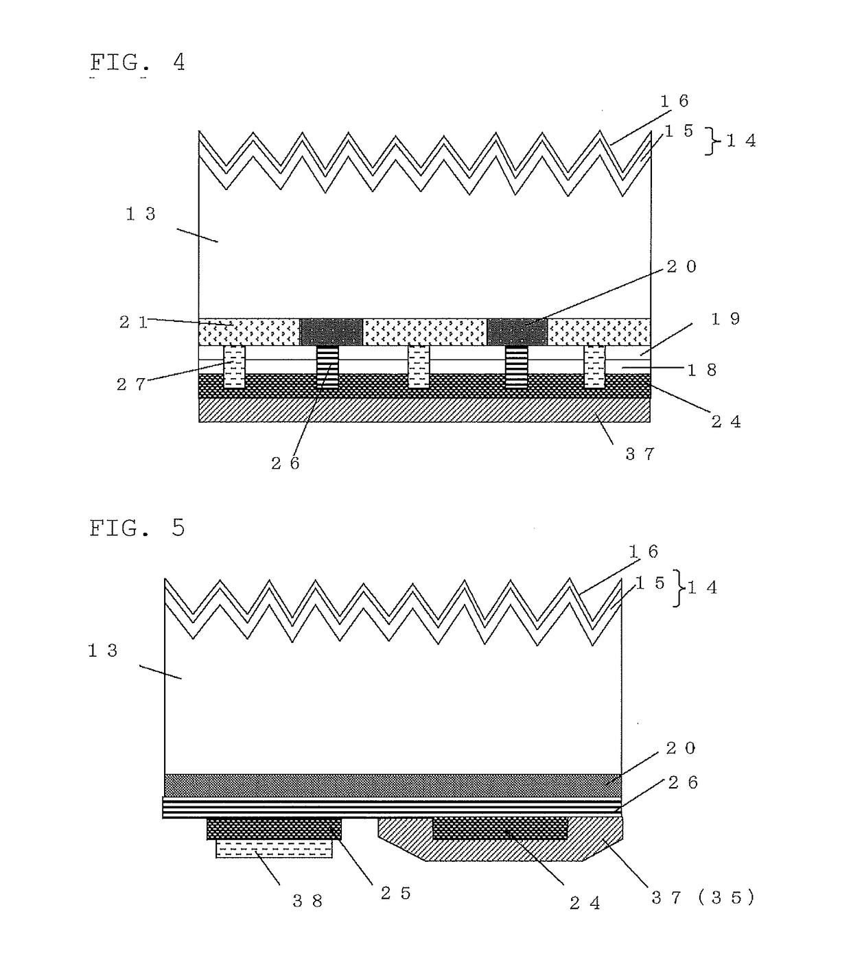
[0135]In Example 1, contact portions, insulator films, current collectors, and bus bar electrodes were formed in a pattern shown in FIGS. 2 and 7 (FIG. 6 (j) to (l)).

[0136]First, contact portions were formed in a pattern of line shapes each having a width of 100 μm. Specifically, conductive paste (sintering paste) composed of Ag particles, glass frit, binder, and solvent was applied onto prescribed portions on the diffusion layer by screen printing. This was dried, and baked at 700° C. for 5 minutes to form first contact portions 26 and second contact portions 27. Then, insulator films each having a width of 3 mm (in the longitudinal direction of the finger electrode) and a length of 150 mm (in the longitudinal direction of the bus bar electrode) were formed just under the bus bar electrodes so as to intersect with the finger electrodes (contact portions) at right angles. As the raw material for the insulator films, polyimide paste was used. This paste was applied onto prescribed pa...


PUM


Abstract

Solar cell including: a semiconductor substrate of a first conductivity type having a region of the first conductivity type and region of a second conductivity type on the back side; a first finger electrode composed of a first contact portion and first current collector, a second finger electrode composed of a second contact portion and second current collector, a first bus bar electrode, a second bus bar electrode on the backside; an insulator film disposed at least in the area just under the first bus bar electrode and second bus bar electrode; wherein the electrical contact between the first current collector and first bus bar electrode as well as electrical contact between the second current collector and the second bus bar electrode are made on the insulator film; and first contact portion and the second contact portion are in a continuous line shape at least just under the insulator film.

Description

TECHNICAL FIELD[0001]The present invention relates to a solar cell and a method for producing thereof.BACKGROUND ART[0002]A previous back surface electrode-type solar cell is schematically shown in FIG. 14 as a cross sectional view. The back surface electrode-type solar cell 210 produced by a previous art will be described by referring to FIG. 14. On the light-receiving surface side of an N-type silicon substrate 213, a rugged shape 214 and an FSF (Front Surface Field) layer 215, which is an N-type diffusion layer, are formed. On the rugged shape 214, a dielectric passivation layer (a surface passivation layer) 217 which contains silicon dioxide and an antireflective film 216 which contains silicon nitride are formed from the side of the N-type diffusion layer 213.[0003]On the backside of the N-type silicon substrate 213, N-type doped N-type diffusion layers 220 and P-type doped P-type diffusion layers 221 are alternately formed. In addition, on the backside of the N-type silicon su...

Claims


Application Information

Patent Timeline
Patent Type & Authority Applications(United States)
IPC IPC(8): H01L31/02H01L31/0216H01L31/068H01L31/0224
CPCH01L31/0201H01L31/068H01L31/02167H01L31/022425H01L31/022433H01L31/022441H01L31/0682Y02E10/547H01L31/02002
Inventor MATSUO, YOKOWATABE, TAKENORIOTSUKA, HIROYUKI
Owner SHIN ETSU CHEM IND CO LTD
Why Eureka
Try Eureka