Display system with capacitive touch panel and manufacturing method thereof

A technology of capacitive touch and display system, which is applied in the direction of electrical digital data processing, input/output process of data processing, instruments, etc., can solve the process steps of capacitive touch panel 100 and the limitation of material selection, and the inability to transmit signals To the problems of metal wires and uneven thickness of the stack layer 110, it can improve the process yield, solve the poor electrical contact, and improve the step coverage.

Inactive Publication Date: 2012-02-08
INNOCOM TECH SHENZHEN +1
View PDF6 Cites 16 Cited by
  • Summary
  • Abstract
  • Description
  • Claims
  • Application Information

AI Technical Summary

Problems solved by technology

[0004] Further, due to the poor step coverage of the stack layer 110, defects (defects) 111 are likely to be formed at the contact interfaces between the two ends of the stack layer 110 and the left electrode 104a and the right electrode 104b, so that the electrical The contact resistance between the stack layer 110 and the indium tin oxide (ITO) layer 104 increases due to poor contact.
Even a disconnected state occurs between the stack layer 110 and the indium tin oxide (ITO) layer 104, so that the left electrode 104a and the right electrode 104b are in an insulated state, and signals cannot be transmitted to the metal wire 106, such as figure 1 shown
[0005] According to the above, due to the uneven thickness of the stack layer 110 and poor electrical contact, it is necessary to carefully select the material of the stack layer 110 and control the thickness of the indium tin oxide (ITO) layer 104 and the dielectric layer 108, so the capacitive The process steps and material selection of the touch panel 100 are very limited
Even if the prior art intends to solve the above-mentioned problems by increasing the thickness of the stacking layer 110, in the process of vapor deposition and lithography, the stacking layer 110 is easily peeled off due to excessive thickness, which still cannot solve the problem of poor step coverage and The problem of poor electrical contact between the stacked layer 110 and the indium tin oxide (ITO) layer 104

Method used


Image

  • Display system with capacitive touch panel and manufacturing method thereof
  • Display system with capacitive touch panel and manufacturing method thereof
  • Display system with capacitive touch panel and manufacturing method thereof

Examples


Embodiment Construction

[0024] The preferred embodiments of the present invention are described in detail by the accompanying drawings and the following descriptions. In different drawings, the same component symbols represent the same or similar components.

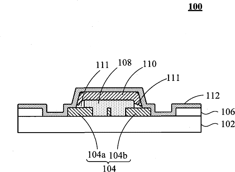
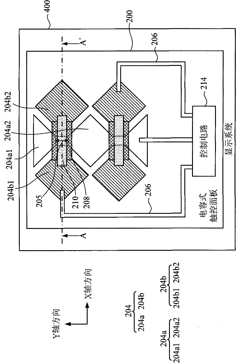
[0025] refer to figure 2 , which shows a top view of the display system 400 with the capacitive touch panel 200 according to the first embodiment of the present invention. A capacitive touch panel (capacitive touch panel) 200 mainly includes a substrate 202, electrode lines 204, a plurality of signal lines 206, a dielectric layer (dielectric layer) 208, an electrode bridge structure 210, and a passivation layer (passivation layer) 212 (marked At Figure 3F ). The electrode circuit 204 is connected to the control circuit 214 through the wire formed by the signal line 206 , and the control circuit 214 is used for processing the sensing signal from the electrode circuit 204 .

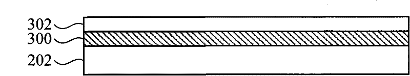
[0026] The electrode circuit 204 is formed on the substrate 202, a...


PUM


Abstract

The invention provides a display system with a capacitive touch panel and a manufacturing method thereof. The display system with a capacitive touch panel comprises a substrate, an electrode circuit, a plurality of signal lines, a dielectric layer and an electrode bridging structure, wherein the electrode circuit is provided with a first electrode and a second electrode, the first electrode comprises a plurality of first conductive patterns, the second electrode comprises a plurality of second patterns, and the first conductive patterns are mutually electrically connected; the plurality of signal lines are formed on the substrate; the dielectric layer is formed on the electrode circuit and covers the electrode circuit; and in the invention, the electrode bridging structure with uniform thickness is formed on the dielectric layer by using a metal open repair technique, so that the second patterns are mutually electrically connected.

Description

【Technical field】 [0001] The present invention relates to a display system and a method thereof, in particular to a display system with a capacitive touch panel and a manufacturing method thereof. 【Background technique】 [0002] refer to figure 1 , which shows a schematic diagram of a capacitive touch panel 100 of a display system in the prior art. The capacitive touch panel 100 includes a substrate 102, an indium tin oxide (ITO) layer 104, a metal wire 106, a dielectric layer (dielectric layer) 108, a stack layer 110 and a passivation layer (passivation layer) 112, the stack Layer 110 is a conductive material. The above-mentioned physical vapor deposition (PVD) method and lithography technology are used to form the indium tin oxide (ITO) layer 104, the dielectric layer 108 and the stack layer 110 in sequence, wherein the indium tin oxide (ITO) layer 104 has a left electrode 104a and a right electrode 104b. [0003] However in figure 1 Among them, near the step edge (st...

Claims


Application Information

Patent Timeline
Patent Type & Authority Applications(China)
IPC IPC(8): G06F3/044
Inventor 陈文龙曾榆钧
Owner INNOCOM TECH SHENZHEN
Why Eureka
Try Eureka