Printed circuit board and manufacturing method thereof

A technology of printed circuit boards and manufacturing methods, which is applied in the direction of printed circuit components, etc., can solve the problems of cumbersome PCB manufacturing process, high product scrap rate, poor impedance pass rate, etc., and achieve high-speed signal transmission performance and impedance pass rate High, low production cost effect

Active Publication Date: 2017-08-25
GUANGZHOU FASTPRINT CIRCUIT TECH +2
View PDF9 Cites 12 Cited by
  • Summary
  • Abstract
  • Description
  • Claims
  • Application Information

AI Technical Summary

Problems solved by technology

However, since there are many factors affecting PCB impedance, and the PCB manufacturing process is relatively cumbersome, the products obtained by traditional methods, especially t...

Method used


Image

  • Printed circuit board and manufacturing method thereof
  • Printed circuit board and manufacturing method thereof
  • Printed circuit board and manufacturing method thereof

Examples


Embodiment Construction

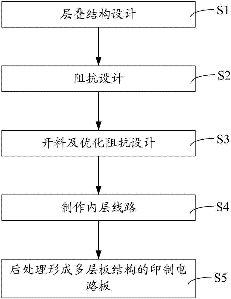
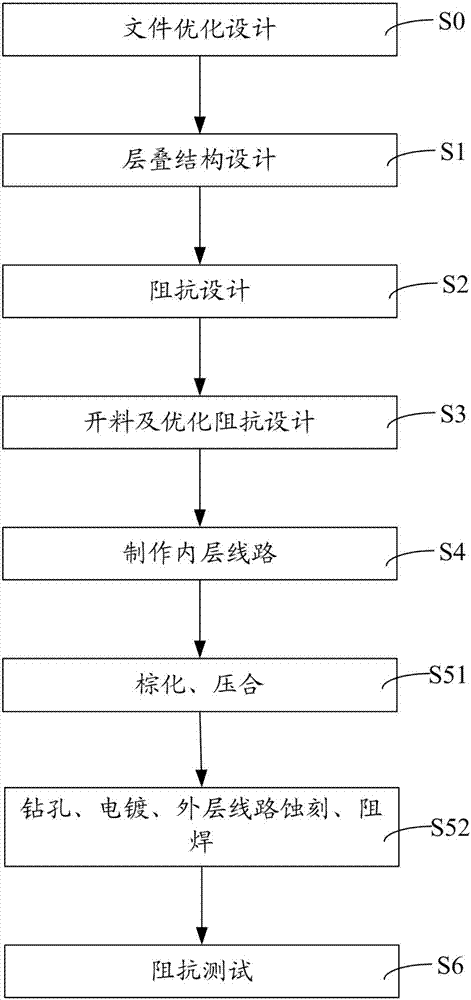
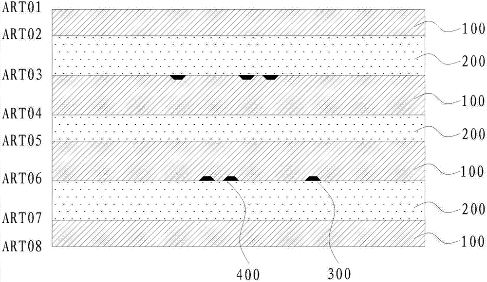
[0034] In order to facilitate the understanding of the present invention, the present invention will be described more fully below with reference to the associated drawings. Preferred embodiments of the invention are shown in the accompanying drawings. However, the present invention can be embodied in many different forms and is not limited to the embodiments described herein. On the contrary, the purpose of providing these embodiments is to make the disclosure of the present invention more thorough and comprehensive.

[0035]It should be noted that when an element is referred to as being “fixed” to another element, it can be directly on the other element or there can also be an intervening element. When an element is referred to as being "connected to" another element, it can be directly connected to the other element or intervening elements may also be present. In contrast, when an element is referred to as being "directly on" another element, there are no intervening elem...


PUM

PropertyMeasurementUnit
Thicknessaaaaaaaaaa

Abstract

The invention discloses a printed circuit board and a manufacturing method thereof. The printed circuit board manufacturing method comprises the following steps: stacked structure design is carried out; impedance design is carried out; cutting and optimized impedance design are carried out; an inner-layer line is manufactured; and a printed circuit board with a multilayer board structure is formed through postprocessing. According to the printed circuit board and the manufacturing method thereof, through monitoring and adjusting factors which influence the impedance value during the cutting and inner-layer line manufacturing production process, the problem that the inner-layer impedance is hard to control caused by each factor during the production process of the printed circuit board can be solved, the inner-layer impedance of the printed circuit board is stably controlled to meet high precision requirements, the high-speed signal transmission performance of the printed circuit board is improved, the impedance qualification rate of the printed circuit board can be further improved, the impedance rejection rate is reduced, the production cost is reduced, and the problem of delivery time delay caused by poor impedance is reduced.

Description

technical field [0001] The invention relates to the technical field of printed circuit boards, in particular to a printed circuit board and a manufacturing method thereof. Background technique [0002] As the PCB (Printed Circuit Board, printed circuit board) tends to develop in the direction of high speed and high frequency, the impedance control precision of the PCB is getting higher and higher. The impedance control accuracy of PCB products is generally ±10%, and some high-end products require impedance control to achieve higher accuracy, such as ±7% or ±5%, and the number of such products is increasing. [0003] Traditionally, when designing the impedance of a PCB, some impedance calculation software is usually used to simulate and predict the impedance, and then select a suitable control scheme according to customer requirements such as stacked structure, line width, and dielectric layer thickness. During production, it is produced according to the control scheme durin...

Claims


Application Information

Patent Timeline
IPC IPC(8): H05K1/02
Inventor 程柳军陈蓓李艳国王红飞
Owner GUANGZHOU FASTPRINT CIRCUIT TECH
Why Eureka
Try Eureka