
Light emitting device and manufacturing method therefor

A technology of light-emitting elements and etching method, which is applied in the direction of electrical components, semiconductor devices, circuits, etc., can solve the problems of reducing light extraction efficiency and poor patterning process, and achieve the goal of improving light extraction efficiency, reducing contact area, and reducing contact area Effect

Inactive Publication Date: 2017-08-29
LUMISTAR S R O
View PDF3 Cites 0 Cited by
  • Summary
  • Abstract
  • Description
  • Claims
  • Application Information

AI Technical Summary

Problems solved by technology

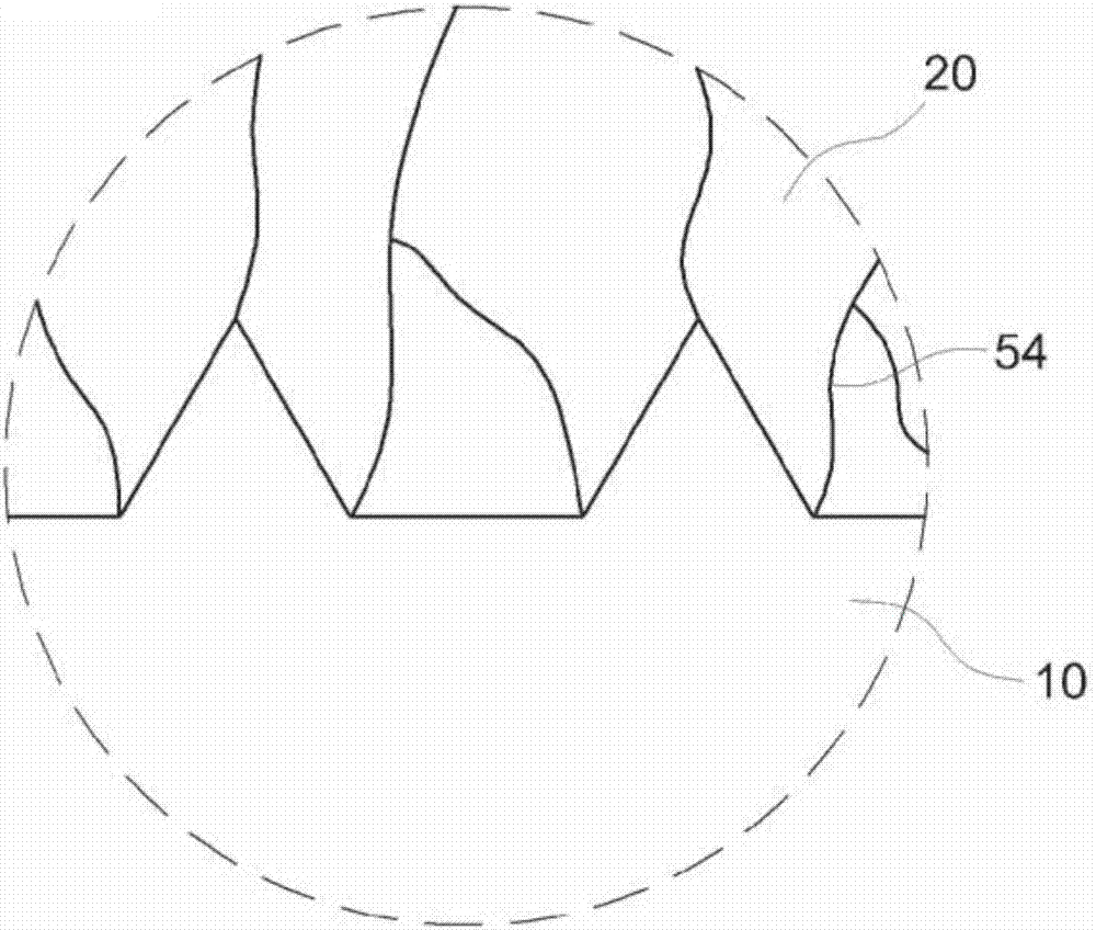
This dislocation acts as a site for light absorption, further reducing light extraction efficiency
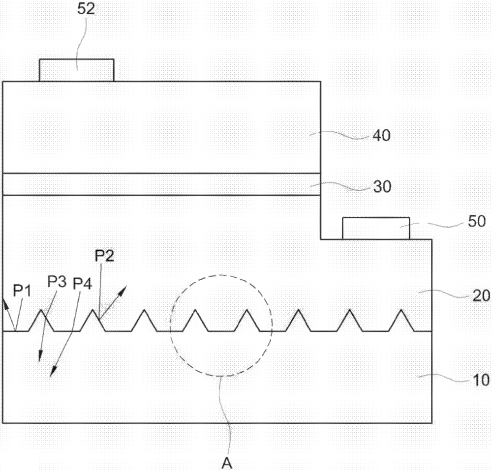
[0013] In addition, when the first conductivity type semiconductor layer 20 is formed through the above-mentioned process, a large amount of heat will be accompanied, and due to the difference in the thermal expansion coefficient between the substrate 10 and the first conductivity type semiconductor layer 20, the first conductivity type semiconductor layer will be caused to shrink. The thermal stress caused by the bending of 20 toward the substrate 10 side not only makes the patterning process of the layers laminated later poor, but also causes a decrease in the light extraction efficiency.

Method used


Image

  • Light emitting device and manufacturing method therefor
  • Light emitting device and manufacturing method therefor
  • Light emitting device and manufacturing method therefor

Examples


Embodiment Construction

[0040] Hereinafter, preferred embodiments of the present invention will be described in detail with reference to the drawings and the contents described later. However, the present invention is not limited to the various embodiments described here, and can be implemented in other ways. On the contrary, various embodiments disclosed herein are provided so that the disclosed contents will be thorough and complete, and can fully convey the idea of ​​the present invention to those skilled in the art. The same reference numerals denote the same constituent elements throughout the specification.

[0041] On the other hand, the terms used in this specification are for explaining an Example, and are not for limiting this invention. In this specification, the plural forms are also included in the singular forms unless otherwise mentioned. In addition, descriptions of positional relationships used in the specification, such as upper, lower, left, right, etc., are described for conveni...


PUM


Abstract

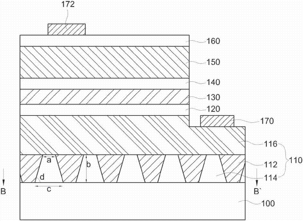
A light emitting device and a method for manufacturing the same are provided. The light emitting device comprises: a substrate; a first conductive semiconductor layer having a first conductive lower semiconductor layer disposed on the substrate and having a void pattern and a first conductive upper semiconductor layer formed on the first conductive lower semiconductor layer; an active layer disposed on the first conductive semiconductor layer; a second conductive semiconductor layer disposed on the active layer; and first and second electrodes which are disposed on the first and second conductive semiconductor layers, respectively, wherein the side walls of the first conductive lower semiconductor layer adjacent to the void pattern are formed in a straight line when seen in a vertical cross-section, and are etched by an inverse slope etching method so that the outer side inclination angle of the side walls with respect to the surface of the substrate overlapping with the void pattern may have an acute angle.

Description

technical field [0001] The present invention relates to a light-emitting element and a manufacturing method thereof, and more particularly to a light-emitting element and a manufacturing method thereof: a semiconductor layer having a low refractive index is formed in a predetermined conductive type semiconductor layer adjacent to a substrate by etching by a reverse gradient etching method. void pattern, thereby improving light extraction efficiency, and helping to minimize stress between the substrate and the semiconductor layer due to crystal incoherence and differences in thermal expansion coefficients. Background technique [0002] A light emitting device (Light Emitting Device) is a device that converts electrical energy into light energy. For example, various colors can be realized by adjusting the composition ratio of compound semiconductors. [0003] Regarding light-emitting elements, when a forward voltage is applied, n-type electrons combine with p-type holes (holes...

Claims


Application Information

Patent Timeline
Patent Type & Authority Applications(China)
IPC IPC(8): H01L33/22H01L33/36H01L33/00
CPCH01L33/00H01L33/22H01L33/36
Inventor 崔有项
Owner LUMISTAR S R O
Learn More