
Full waveguide lateral polysilicon optical interconnection system based on standard cmos process

A polysilicon, optical interconnect technology, applied in semiconductor devices, electrical components, circuits, etc., can solve the problems of design structure loss, energy loss, low luminous efficiency, etc., to reduce energy loss, increase responsivity, and improve responsivity. Effect

Inactive Publication Date: 2020-08-14
TIANJIN UNIV
View PDF5 Cites 0 Cited by
  • Summary
  • Abstract
  • Description
  • Claims
  • Application Information

AI Technical Summary

Problems solved by technology

However, the problem of low luminous efficiency of PN junction light-emitting devices has always been difficult to solve.
The reason is not only the low luminous efficiency of Si-based PN-LED itself, but also a lot of loss in the design structure: first, Si-LED emits light as a junction formed by a high-doped junction and a low-doped well, and the part that can be measured and seen externally Only the side PN junction emits upward light, while the light emitted by other parts is absorbed by the bulk silicon and cannot be used as a transmission signal, resulting in serious energy loss; secondly, the general CMOS process will cover the silicon surface with an oxide layer, because the silicon PN-LED emits The light is incident from Si to SiO 2 , while the refractive index of silicon is lower than that of SiO 2 The refractive index is much larger, which causes a large part of the light emitted by the bulk silicon LED to be unable to be transmitted due to the total reflection effect.

Method used


Image

  • Full waveguide lateral polysilicon optical interconnection system based on standard cmos process
  • Full waveguide lateral polysilicon optical interconnection system based on standard cmos process
  • Full waveguide lateral polysilicon optical interconnection system based on standard cmos process

Examples


Embodiment Construction

[0034] The full-waveguide lateral polysilicon optical interconnection system based on the standard CMOS process of the present invention will be described in detail below with reference to the embodiments and the accompanying drawings.

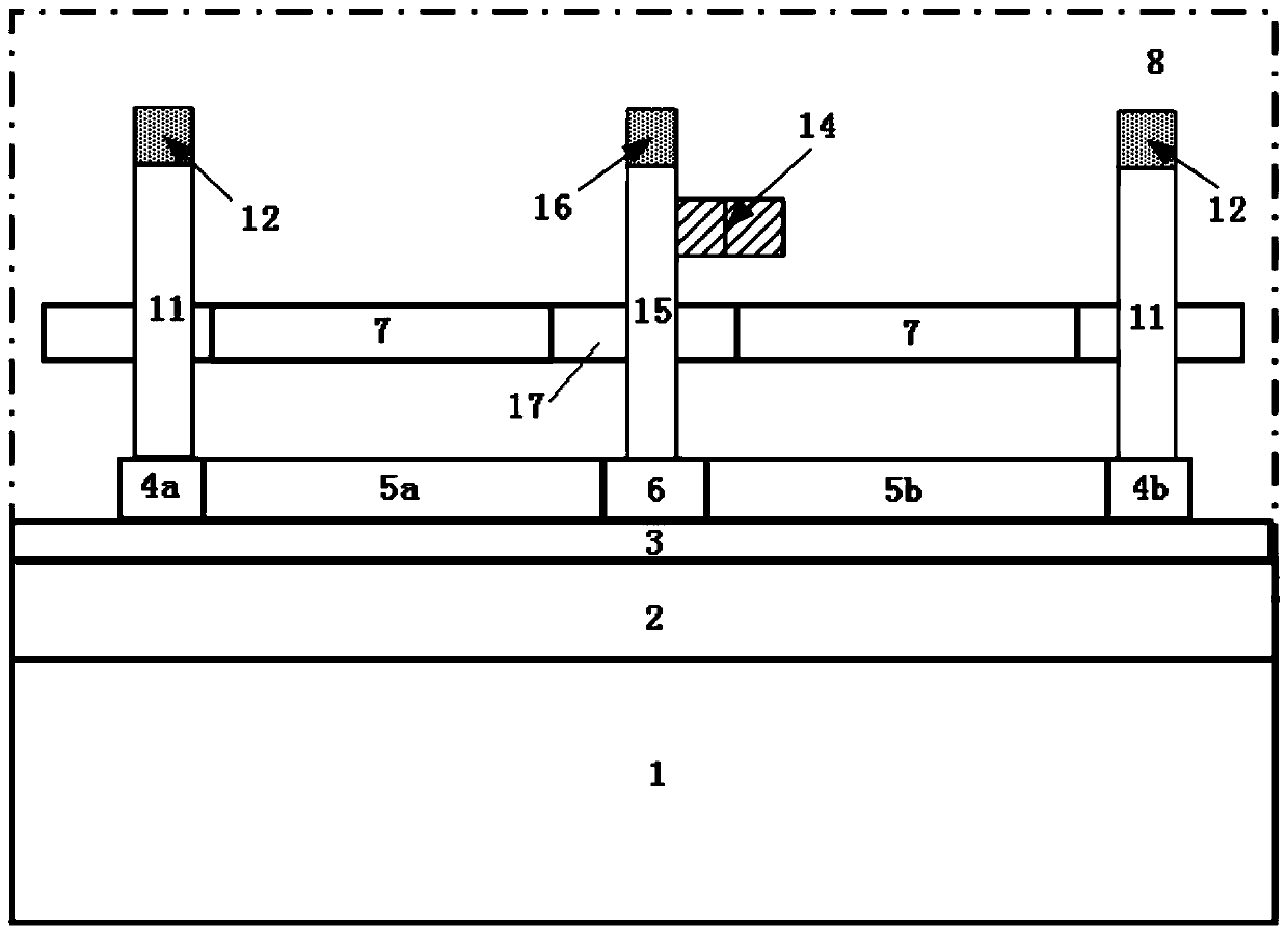
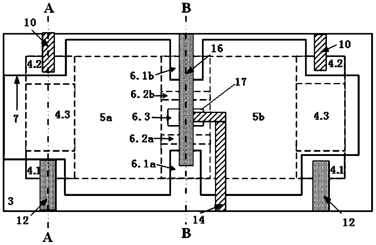
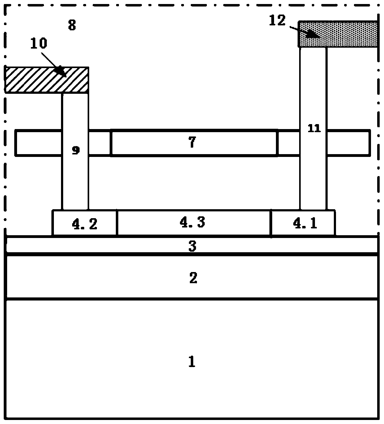
[0035] like figure 1As shown, the full-waveguide lateral polysilicon optical interconnection system based on the standard CMOS process of the present invention includes a P-Sub substrate 1, a shallow trench isolation (field oxygen) layer 2 and a gate oxide layer 3 arranged in sequence from bottom to top , the upper end surface of the gate oxide layer 3 is provided with SiO 2 isolation layer 8, the SiO 2 The isolation layer 8 is respectively embedded with: an optical interconnection layer located on the upper end of the gate oxide layer 3 and a metal light reflection plate 7 located above the optical interconnection layer, wherein the optical interconnection layer includes a The first polysilicon photodetector 4a, the first polysilicon optica...


PUM


Abstract

The invention discloses a standard CMOS technology-based full-waveguide transverse polysilicon optical interconnection system, which comprises a substrate, a shallow channel isolation layer and a gateoxide layer which are sequentially arranged from bottom to top, wherein a SiO2 layer is arranged on the upper end surface of the gate oxide layer; an optical interconnection layer located at the upper end of the gate oxide layer and a metal light reflection plate located at the upper part of the optical interconnection layer are embedded into the SiO2 layer separately, wherein the optical interconnection layer comprises a first polysilicon photoelectric detector, a first polysilicon optical waveguide, a polysilicon LED group, a second polysilicon optical waveguide and a second polysilicon photoelectric detector which are sequentially arranged from left to right; a plurality of connecting line holes for connecting the first polysilicon photoelectric detector, the second polysilicon photoelectric detector, the polysilicon LED group and an external power supply, and an external wire penetrating through the connecting line holes are also embedded into a SiO2 isolation layer; and a wire through hole or wire through groove through which the external wire penetrates is formed in the metal light reflection plate. According to the standard CMOS technology-based full-waveguide transverse polysilicon optical interconnection system, an optical signal is emitted by fully utilizing LEDs, so that the responsivity of the optical interconnection system is improved and the energy loss is reduced.

Description

technical field [0001] The invention relates to an all-waveguide lateral polysilicon optical interconnection system. In particular, it relates to a full-waveguide lateral polysilicon optical interconnection system based on a standard CMOS process. Background technique [0002] With the rapid development of science and technology, microelectronic products are developing towards small and precise. In the 21st century, the development of microelectronics has encountered the bottleneck of physical limits. Further scaling down through "Moore's Law" would not only dramatically increase manufacturing costs, but also lead to undesired physical effects. Another more pressing bottleneck is the delay and power consumption of electrical interconnections within microelectronic chips. With the increase of integration, the delay of individual transistors is getting smaller and smaller, but the delay of interconnect lines is getting larger, and the reduction of interconnect size increase...

Claims


Application Information

Patent Timeline
Patent Type & Authority Patents(China)
IPC IPC(8): H01L27/04
CPCH01L27/04
Inventor 毛陆虹丛佳谢生郭维廉
Owner TIANJIN UNIV
Learn More