Computer-implemented method and terminal equipment for semiconductor device design

A device design and implementation method technology, applied in the direction of design optimization/simulation, special data processing applications, etc., can solve problems such as low efficiency of control codes, reduce the technical threshold of editing and modification, and improve editing efficiency.

Active Publication Date: 2021-04-09
SHANGHAI MI FANG ELECTRONICS LTD
View PDF1 Cites 0 Cited by
  • Summary
  • Abstract
  • Description
  • Claims
  • Application Information

AI Technical Summary

Problems solved by technology

[0004] In view of this, the embodiment of the present application provides a computer-implemented method and terminal equipment for semiconductor devic

Method used


Image

  • Computer-implemented method and terminal equipment for semiconductor device design
  • Computer-implemented method and terminal equipment for semiconductor device design
  • Computer-implemented method and terminal equipment for semiconductor device design

Examples


Example Embodiment

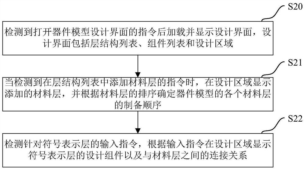
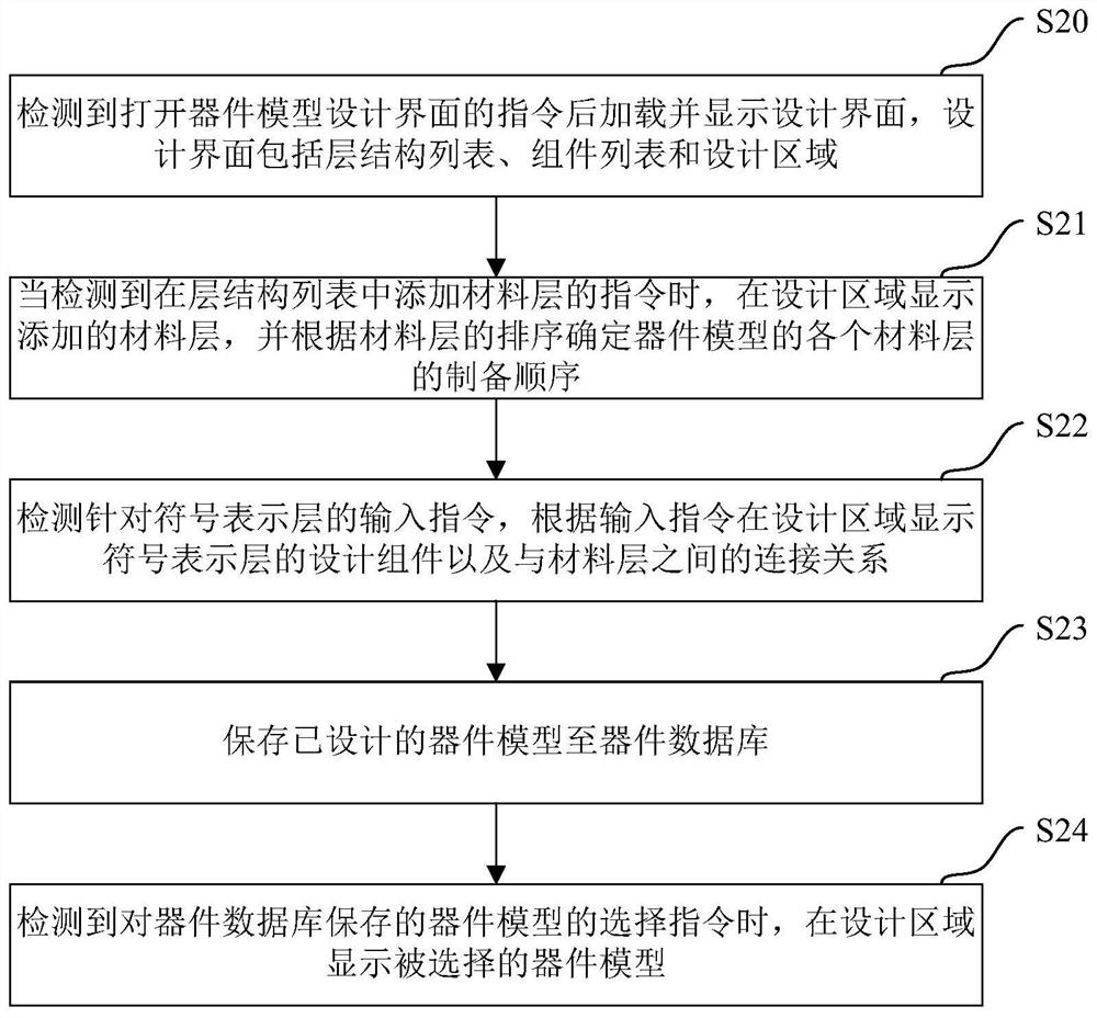
[0014] The present application is described below based on examples, but the present application is not limited to these examples only. In the following detailed description of the application, some specific details are described in detail. Those skilled in the art can fully understand the present application without the description of these detailed parts. Well-known methods, procedures, procedures, components and circuits have not been described in detail in order to avoid obscuring the essence of this application.

[0015] Furthermore, those of ordinary skill in the art will appreciate that the drawings provided herein are for illustrative purposes and are not necessarily drawn to scale.

[0016] Meanwhile, it should be understood that in the following description, "circuit" refers to a conductive loop formed by at least one element or sub-circuit through electrical connection or electromagnetic connection. When an element or circuit is referred to as being "connected" to...


PUM


Abstract

The present application provides a computer implementation method and terminal equipment for semiconductor device design, including: loading and displaying the design interface after detecting an instruction to open the device model design interface, the design interface includes a layer structure list, a component list and a design area, wherein, The layer structure list includes the symbol representation layer and material layer of the device model, the component list includes the design components used in the layer structure, and the design area is used to display the layer structure and design components of the device model; when it is detected that the material is added in the layer structure list When specifying layers, display the added material layers in the design area, and determine the preparation sequence of each material layer of the device model according to the order of the material layers; you can also change the representation method of semiconductor devices and the manufacturing properties of materials in the design area according to the input instructions .

Description

technical field [0001] The present application relates to the field of semiconductor devices, in particular to a computer-implemented method and terminal equipment for semiconductor device design. Background technique [0002] Semiconductor devices are used in various electronic devices such as personal computers, cell phones, digital cameras, and other electronic devices. With the continuous development of computer and simulation technology, simulation design technology has played an increasingly important role in supporting the development of the semiconductor device industry. With the gradual maturity of 3D printing technology, it is possible to prepare semiconductor devices by printing. [0003] Developers will be able to control the process of 3D printing semiconductor devices through programming, and will also face a large number of printing requirements due to circuit design needs, so many printing algorithms need to be developed to meet each printing requirement. I...

Claims


Application Information

Patent Timeline
IPC IPC(8): G06F30/20
CPCG06F30/20
Inventor 黄寿魁
Owner SHANGHAI MI FANG ELECTRONICS LTD
Why Eureka
Try Eureka