Array substrate, display module and electronic equipment

An array substrate and display module technology, applied in the electronic field, can solve problems such as limited identification area of ​​fingerprint identification modules, increased difficulty in structural design of electronic products, and high requirements for chip production capacity, so as to simplify the structural design of electronic equipment and reduce the design cost. Difficulty, the effect of increasing the fingerprint recognition area

Inactive Publication Date: 2017-09-08
SHANGHAI YUDE TECH CO LTD
View PDF4 Cites 13 Cited by
  • Summary
  • Abstract
  • Description
  • Claims
  • Application Information

AI Technical Summary

Problems solved by technology

[0003] The inventors of the present invention found in the process of realizing the present invention that fingerprint recognition and iris recognition in electronic products are mostly independent functional modules, which communicate with the main chip through circuit connection to realize corresponding functions, and such independent fingerprint recognition Recognition and iris recognition function modules have complex structures and generally require openings, which increases the difficulty of structural design of electronic products, and the recognition area of ​​the independent fingerprint recognition module is limited, causing inconvenience for users
At the same time, the independent fingerprint recognition module and iris recognition module each need to manufacture a sensory chip separately, which requires high chip production capacity and high cost

Method used


Image

  • Array substrate, display module and electronic equipment
  • Array substrate, display module and electronic equipment
  • Array substrate, display module and electronic equipment

Examples


Embodiment Construction

[0027] In order to make the object, technical solution and advantages of the present invention clearer, various embodiments of the present invention will be described in detail below in conjunction with the accompanying drawings. However, those of ordinary skill in the art can understand that, in each implementation manner of the present invention, many technical details are provided for readers to better understand the present application. However, even without these technical details and various changes and modifications based on the following implementation modes, the technical solution claimed in this application can also be realized.

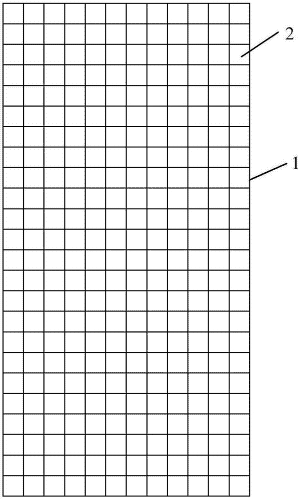
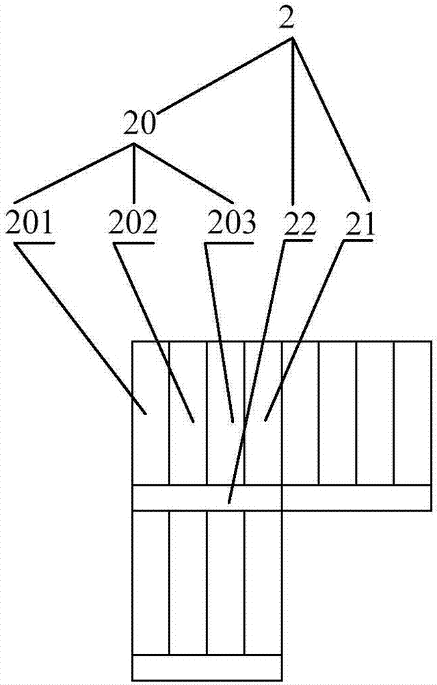
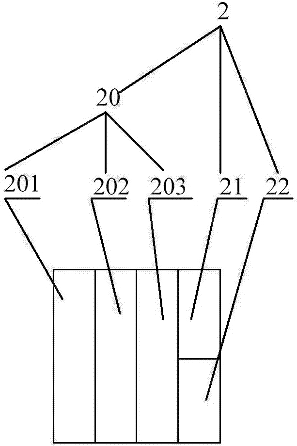
[0028] The first embodiment of the present invention relates to an array substrate, which is applied in a display module. Wherein, the display module can be an AMOLED (Active Matrix / Organic Light Emitting Diode, active matrix organic light emitting diode) display module, an LCD (Liquid Crystal Display, liquid crystal display) display module...


PUM


Abstract

The invention relates to the technical field of electronics, and discloses an array substrate, a display module and electronic equipment. The array substrate comprises a substrate body and first basic points which are in matrix arrangement on the substrate body; the first basic points comprise M display pixels, M infrared sensing units and N infrared light emitting units which are arranged together, wherein M and N are both positive integers, and M is greater than or equal to N; and the substrate body also has signal circuits of the display pixels, the infrared light emitting units and the infrared sensing units. According to the embodiments, by integrating the infrared light emitting units, the infrared sensing units and the display pixels of the display apparatus together, the structural design difficulty of the electronic equipment can be lowered and open pores can be reduced; in addition, the infrared sensing units can be used for fingerprint identification as well as iris identification, so that multifunction is realized and cost can be lowered; and meanwhile, the fingerprint identification function is realized in a display region, so that fingerprint identification flexibility is improved, and convenience in use of a user can be achieved.

Description

technical field [0001] The invention relates to the field of electronic technology, in particular to an array substrate, a display module and electronic equipment. Background technique [0002] Biometric identification functions (such as fingerprint identification and iris identification) are widely used in electronic products. Most of the existing fingerprint identification schemes are based on the capacitive principle (it uses semiconductor capacitor array sensing to measure the capacitance change of each pixel point, each pixel point is a capacitive electrode, when the finger is pressed on the fingerprint module identification area, according to the fingerprint The difference in the capacitance value of the valley and the fingerprint ridge realizes the fingerprint recognition function). At present, the fingerprint module of the mobile phone is generally arranged at the position of the front button, and such a fingerprint module generally has a cover plate. Due to the li...

Claims


Application Information

Patent Timeline
Patent Type & Authority Applications(China)
IPC IPC(8): G06K9/00G06F3/041
CPCG06F3/0412G06V40/1318G06V40/19
Inventor 杨朝蓉黄青青徐娜
Owner SHANGHAI YUDE TECH CO LTD
Why Eureka
Try Eureka