Two-sided core plate structure used for BOT packaging and manufacturing method therefor

A core board, double-sided technology, applied in the double-sided core board structure and its manufacturing field, can solve the problems of large bonding force, inability to use core board, embedded circuit technical limitations, etc., and achieves small 3D packaging size and packaging density. Large, highly integrated effects

Active Publication Date: 2017-09-08
NAT CENT FOR ADVANCED PACKAGING
View PDF4 Cites 9 Cited by
  • Summary
  • Abstract
  • Description
  • Claims
  • Application Information

AI Technical Summary

Problems solved by technology

It can only be applied to the processing and manufacturing of coreless substrates, and can only be used for the first layer of circuits, and cannot be used for circuits after the first layer. Therefore, BOT technology can only be processed on one side of the substrate
Buried line technology is therefore very limited in application
[0006] Since the conven

Method used


Image

  • Two-sided core plate structure used for BOT packaging and manufacturing method therefor
  • Two-sided core plate structure used for BOT packaging and manufacturing method therefor
  • Two-sided core plate structure used for BOT packaging and manufacturing method therefor

Examples


Embodiment Construction

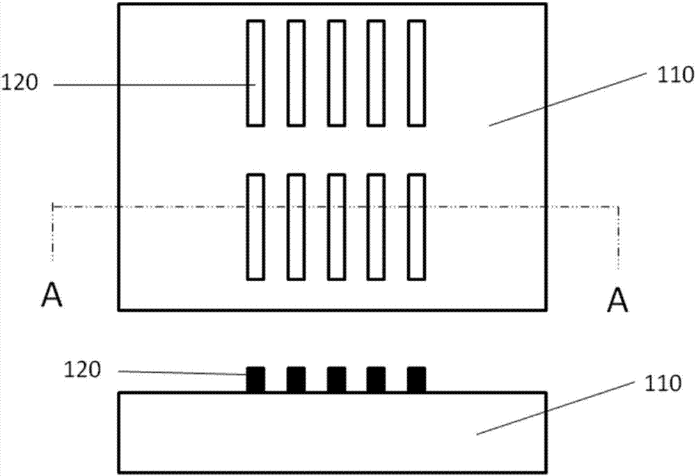
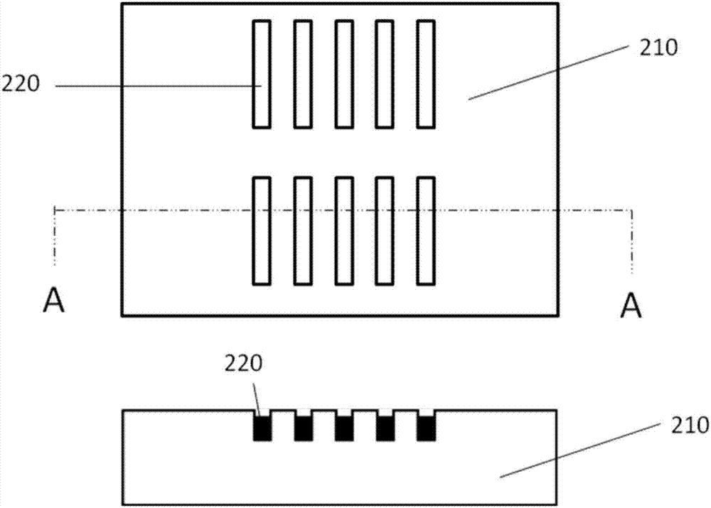
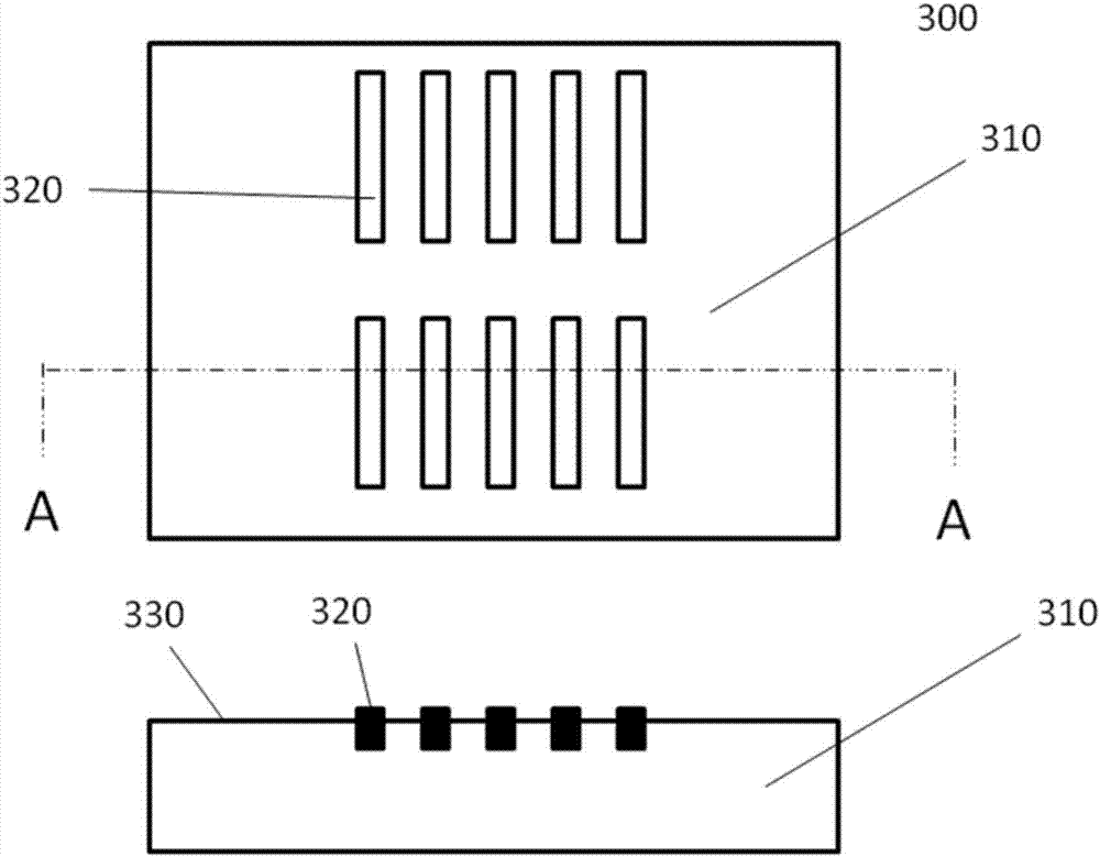
[0039] In the following description, the present invention is described with reference to various examples. However, one skilled in the art will recognize that the various embodiments may be practiced without one or more of the specific details, or with other alternative and / or additional methods, materials, or components. In other instances, well-known structures, materials, or operations are not shown or described in detail so as not to obscure aspects of the various embodiments of the invention. Similarly, for purposes of explanation, specific quantities, materials and configurations are set forth in order to provide a thorough understanding of embodiments of the invention. However, the invention may be practiced without these specific details. Furthermore, it should be understood that the various embodiments shown in the drawings are illustrative representations and are not necessarily drawn to scale.

[0040] In this specification, reference to "one embodiment" or "the ...


PUM


Abstract

An embodiment of the invention provides a two-sided core plate structure. The two-sided core plate structure comprises at least two layers semi-cured substrates on the two surfaces of the two-sided core plate structure, semi-embedded circuits which are semi-embedded in the semi-cured substrates, and a solder resisting layer, wherein the first surfaces of the semi-embedded circuits are positioned above the surfaces of the semi-cured substrates on the same side of the circuits; the second surfaces, opposite to the first surfaces, of the semi-embedded circuits are positioned below the surfaces of the semi-cured substrates on the same side of the circuits; one parts of the side surfaces of the semi-embedded circuits are positioned above the surfaces of the semi-cured substrates on the same side of the circuits; the other parts of the side surfaces of the semi-embedded circuits are coated with the semi-cured substrates; the solder resisting layer at least partially covers the surfaces of the semi-embedded circuits, and exposes a bonding pad window.

Description

technical field [0001] The invention relates to the field of semiconductor packaging, in particular to a double-sided core board structure for BOT packaging and a manufacturing method thereof. Background technique [0002] In order to meet the increasingly miniaturized, intelligent, high-performance and high-reliability development of electronic products, the miniaturization and intelligence of chips have led to an increase in the number of chip package pins, and the size of package pins is also rapidly increasing. At the same time, SiP (System In a Package) requires multiple active electronic components with different functions and optional passive devices to be packaged into a functional system, which proposes the realization of multiple Packaging requirements for a high-performance chip. [0003] When the chip pad spacing of the chip is less than 50 μm, the package must adopt BOT (Bump on Trace) technology to directly bond the copper pillar bumps on the chip surface to t...

Claims


Application Information

Patent Timeline
IPC IPC(8): H01L23/498H01L21/48
Inventor 于中尧
Owner NAT CENT FOR ADVANCED PACKAGING
Why Eureka
Try Eureka