Image Sensor Structure and Method of Forming the Same

An image sensor and doping concentration technology, applied in the direction of electric solid-state devices, semiconductor devices, electrical components, etc., can solve the problem that the photodiode does not have a strong enough electric field and takes a long time

Pending Publication Date: 2021-04-09
SILICON OPTRONICS
View PDF0 Cites 2 Cited by
  • Summary
  • Abstract
  • Description
  • Claims
  • Application Information

AI Technical Summary

Problems solved by technology

At this time, the potential of the photodiode will be too flat, so that the photodiode does not have a strong enough electric fi

Method used


Image

  • Image Sensor Structure and Method of Forming the Same
  • Image Sensor Structure and Method of Forming the Same
  • Image Sensor Structure and Method of Forming the Same

Examples


Embodiment Construction

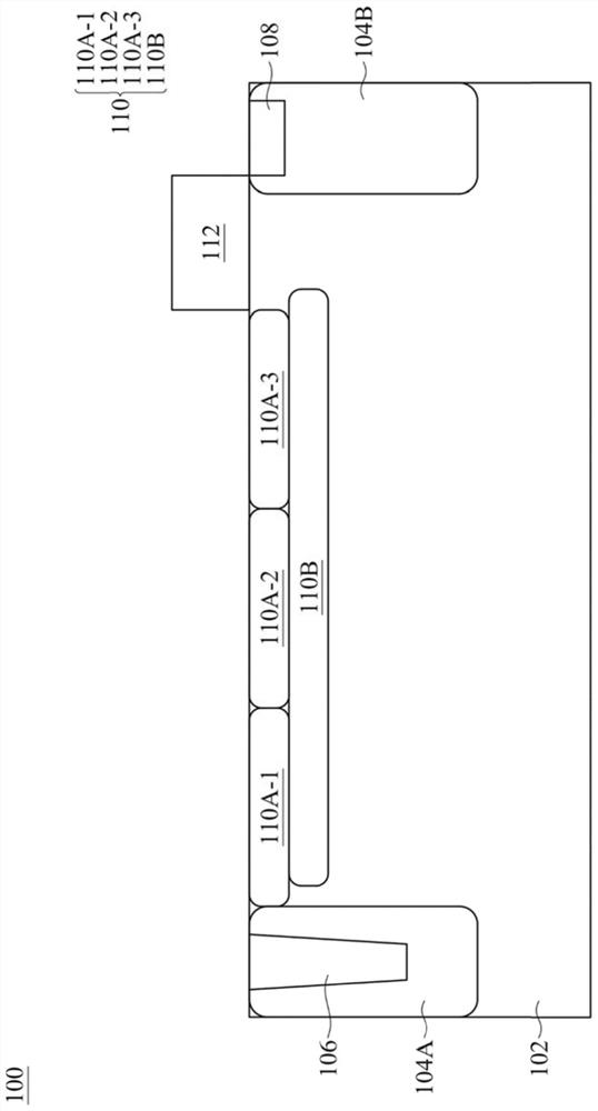
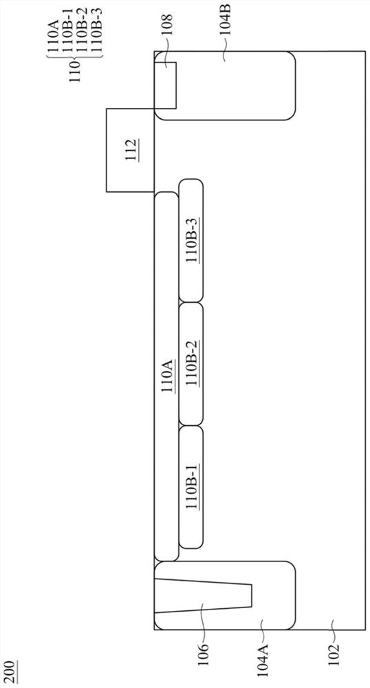
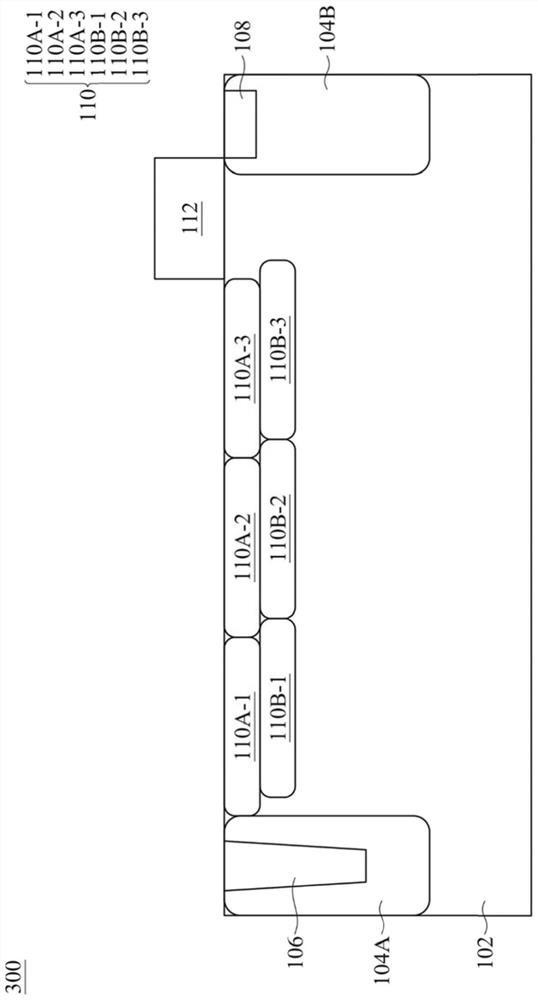
[0036] The structure of the image sensor and its forming method of the embodiments of the present invention will be described in detail below. It should be understood that the following description provides many different embodiments or examples for implementing different aspects of the embodiments of the present invention. The specific elements and arrangements described below are merely to briefly and clearly describe some embodiments of the present invention. Of course, these are only examples rather than limitations of the present invention. In addition, similar and / or corresponding symbols may be used in different embodiments to denote similar and / or corresponding elements, so as to clearly describe the embodiments of the present invention. However, the use of these similar and / or corresponding symbols is only used to briefly and clearly describe some embodiments of the present invention, and does not mean that there is any relationship between the different embodiments ...


PUM


Abstract

The invention provides an image sensor structure and a method of forming the same. The image sensor structure including: a substrate, having a first conductive type; a first well region and a second well region disposed in the substrate and spaced apart; an isolation region disposed in the first well region; a gate disposed on the substrate and between the first well region and the second well region; and a pinned photodiode disposed in the substrate and between the first well region and the second well region is provided. The pinned photodiode includes: a first doping region disposed in the substrate and having a first doping concentration and the first conductive type; and a second doping region disposed under the first doping region and having a second doping concentration and a second conductive type opposite to the first conductive type. One or both of the first doping concentration and the second doping concentration are non-uniform and the first doping concentration is greater than the second doping concentration.

Description

technical field [0001] Embodiments of the present invention relate to an image sensor structure and its forming method, and in particular to an image sensor structure with pinned photodiodes and its forming method. Background technique [0002] Image sensors have been widely used in various image capture devices, such as video cameras, digital cameras and the like. An image sensor, such as a charge-coupled device (CCD) image sensor or a complementary metal-oxide semiconductor (CMOS) image sensor, has a photosensitive element for converting incident light into an electrical signal. The image sensor has a pixel array, and each pixel has a photosensitive element. Image sensors also have logic circuits for transmitting and processing electrical signals. [0003] While existing image sensors generally serve their intended purpose, they are not yet perfect in every respect. For example, when the pixel size is larger, the length of the photodiode will also be longer. At this t...

Claims


Application Information

Patent Timeline
IPC IPC(8): H01L27/146
CPCH01L27/1461H01L27/14643H01L27/14683H01L27/1463H01L27/14612H01L27/14616
Inventor 李明祥李柏叡姚裕源
Owner SILICON OPTRONICS
Why Eureka
Try Eureka