A Lateral Insulated Gate Bipolar Transistor
A bipolar transistor and insulated gate technology, applied in the direction of transistors, diodes, semiconductor devices, etc., can solve the problems of weakening the conductance modulation effect in the drift region, unfavorable practical application of devices, increasing forward conduction voltage drop, etc., and achieving low conduction Effect of voltage drop, high breakdown voltage, fast turn-off speed
- Summary
- Abstract
- Description
- Claims
- Application Information
AI Technical Summary
Problems solved by technology
Method used
Image
Examples
Embodiment 1
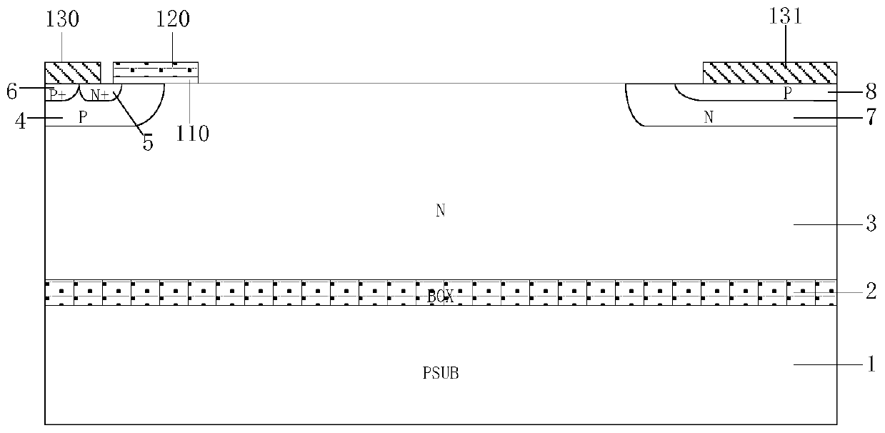
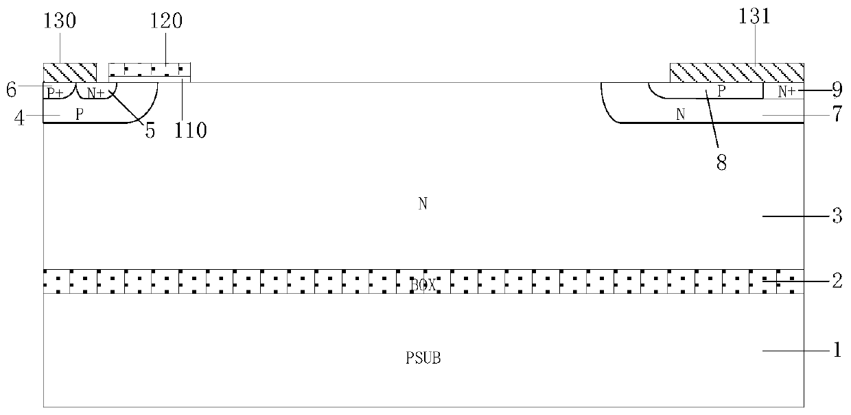
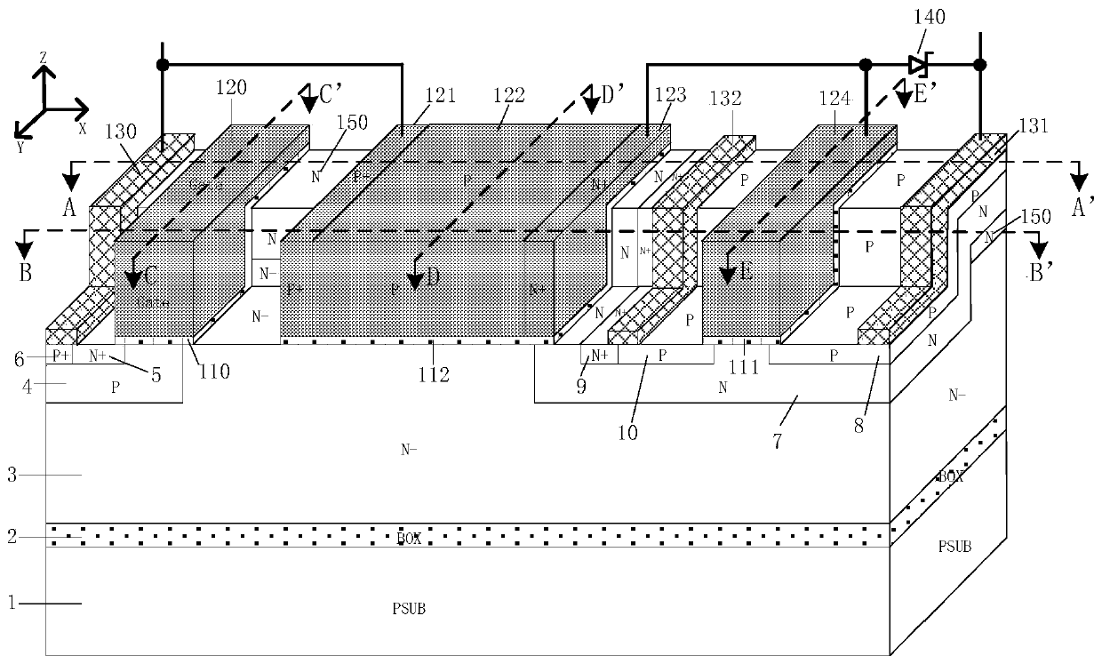
[0035] Such as image 3 As shown, it is a schematic structural diagram of this example, and its half-cell structure includes a substrate 1, an insulating layer 2, and a first N-type low-doped region 3 stacked in sequence from bottom to top; it is characterized in that, along the longitudinal direction of the device, The first N-type low-doped region 3 is in the shape of a two-level ladder, and the vertical height of the second-level step is defined to be greater than the first-level step. Both sides of the upper layer of the first N-type low-doped region 3 have P-type bodies respectively. Region 4 and N-type buffer zone 7, along the longitudinal direction of the device, the P-type body region 4 and N-type buffer zone 7 are two-level ladder; in the first N-type low-doped region 3 second-level ladder and P There is a second N-type low-doped region 150 between the second level of the N-type body region 4 and the N-type buffer zone 7; the upper layer of the P-type body region 4 ha...
Embodiment 2
[0042] Such as Figure 9 As shown, different from Example 1,
[0043] A zener diode is directly formed in the polysilicon layer above the dielectric layer 112, the zener diode is formed on the device surface between the trenches, the P+ region 125 is the anode of the zener diode, and the N+ region 126 is the cathode of the zener diode . The type, location and shape of the Zener diodes can be adjusted as desired.
Embodiment 3
[0045] Such as Figure 10 As shown, the difference from Embodiment 1 is that a Zener diode is directly formed in the polysilicon layer above the dielectric layer 111, and the Zener diode is formed on the surface of the device between the trenches, and the P+ region 125 is a Zener diode The anode of the N+ region 126 is the cathode of the Zener diode. The type, location and shape of the Zener diodes can be adjusted as desired.
PUM
 Abstract
Description
Claims
Application Information


