Method for manufacturing non-punch-through (NPT) type groove IGBT (Insulated Gate Bipolar Transistor) with field stop structure

A non-punch-through, manufacturing method technology, used in semiconductor/solid-state device manufacturing, electrical components, circuits, etc., can solve the problems of difficult ohmic contact and large area, and achieve fast switching speed, excellent performance, and easy processing technology. Effect

Inactive Publication Date: 2011-09-14
TIANJIN HUANXIN TECH DEV
View PDF4 Cites 9 Cited by
  • Summary
  • Abstract
  • Description
  • Claims
  • Application Information

AI Technical Summary

Problems solved by technology

Since the terminal structure formed by the patented manufacturing method uses metal to contact the lightly doped P-main junction, it is difficult to form a good ohmic contact between the metal and the P-main junction; in addition, the terminal structure formed by this manufacturing method only has The main junction terminal structure, in the case of achieving the same withstand voltage, the area is too large

Method used


Image

  • Method for manufacturing non-punch-through (NPT) type groove IGBT (Insulated Gate Bipolar Transistor) with field stop structure
  • Method for manufacturing non-punch-through (NPT) type groove IGBT (Insulated Gate Bipolar Transistor) with field stop structure
  • Method for manufacturing non-punch-through (NPT) type groove IGBT (Insulated Gate Bipolar Transistor) with field stop structure

Examples


Embodiment Construction

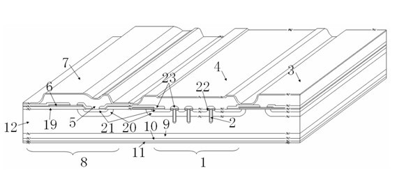
[0041] Below in conjunction with accompanying drawing, the present invention will be further described: with reference to Figure 1 to Figure 8 , the IGBT manufacturing method of the present invention has the following steps:

[0042] (1) Clean the silicon substrate, form a field silicon oxide insulating dielectric film 19 with a thickness of 1~2um on the upper surface of the silicon substrate through the first thermal oxidation growth, photolithography, and then etch the field silicon oxide The insulating dielectric film forms the cell region 1 and the voltage-resistant ring region 8, and forms one or more field-limiting ring injection regions 5 in the voltage-resistant ring region 8;

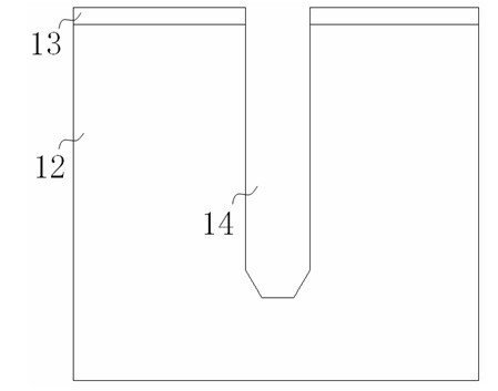
[0043] (2) Deposit a layer of silicon oxide insulating dielectric film 13 on the upper surface of the silicon substrate, remove the silicon oxide insulating dielectric film 13 at the position of the trench 14, and use the unetched silicon oxide insulating dielectric film 13 as a mask film etc...


PUM


Abstract

The invention discloses a method for manufacturing a non-punch-through (NPT) type groove IGBT (Insulated Gate Bipolar Transistor) with a field stop structure, and the method comprises the following steps: in a groove at a surface celluar area on a silicon chip, based on a silicon nitride insulating medium membrane serving as groove side wall protection, forming a thick silicon oxide insulating medium membrane at the bottom of the groove by twice thermal oxide growth, and forming a thin silicon oxide insulating medium membrane at the side wall of the groove by once thermal oxide growth; forming a composite field limiting ring outside a celluar area through twice ion implantation and thermal treatment, forming a composite field plate through polycrystalline silicon, metal deposition and corrosion, and forming one or more pressure rings by the composite field limiting ring and the composite field plate; and at the lower surface of the silicon chip, forming a field stop layer and a current collector region through twice ion implantation and shallow junction thermal treatment. The determined manufacturing method is low in cost and easy to implement; the manufactured IGBT area is small, the switching speed is fast, and the IGBT manufactured by the method has the performance characteristics of low power consumption, enhanced anti-electromagnetic interference and radiation-resistance capability, and the like, thus meeting the demand of the market on high quality of IGBT products.

Description

technical field [0001] The invention relates to an IGBT (insulated gate bipolar transistor) manufacturing method in the field of power devices, in particular to a non-penetrating trench IGBT manufacturing method with a field stop structure. Background technique [0002] IGBT, or Insulated Gate Bipolar Transistor, is a device composed of a MOSFET (Field Effect Transistor) and a bipolar transistor. It includes an NMOS field effect transistor and a PNP bipolar transistor driven by the NMOS field effect transistor; or includes a PMOS field effect transistor and an NPN bipolar transistor driven by the PMOS field effect transistor, NMOS field effect transistor or PMOS The field effect transistor includes an emitter electrode, a gate electrode and a silicon substrate body region, and a PNP bipolar transistor or an NPN transistor includes an emitter electrode, a silicon substrate body region and a collector electrode. [0003] IGBT is mainly used in industrial control, consumer ele...

Claims


Application Information

Patent Timeline
Patent Type & Authority Applications(China)
IPC IPC(8): H01L21/331
Inventor 饶祖刚丛培金沈浩平冯春阳陆界江赵雁
Owner TIANJIN HUANXIN TECH DEV
Why Eureka
Try Eureka