Planar gate IGBT device with deep trench electric field shielding structure

A technology of electric field shielding and planar grid, which is applied in the direction of electrical components, semiconductor devices, circuits, etc., can solve the problems of limited concentration of CSL layer, small short-circuit safe working area, and excessive gate drive charge, so as to improve the safe working area, Enhancement effect, effect of low saturation current density

Active Publication Date: 2019-05-07
UNIV OF ELECTRONICS SCI & TECH OF CHINA
View PDF3 Cites 9 Cited by
  • Summary
  • Abstract
  • Description
  • Claims
  • Application Information

AI Technical Summary

Problems solved by technology

[0004] The object of the present invention is to propose a novel carrier storage layer for the problems of excessive gate drive charge, small short-circuit safe working area and limited CSL layer concentration of the existing slot gate IGBT with carrier storage layer. Planar Gate IGBT

Method used


Image

  • Planar gate IGBT device with deep trench electric field shielding structure
  • Planar gate IGBT device with deep trench electric field shielding structure
  • Planar gate IGBT device with deep trench electric field shielding structure

Examples


Embodiment 1

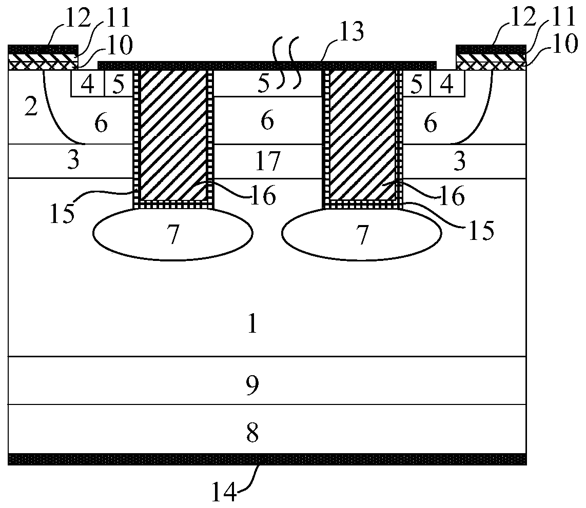
[0030] This embodiment provides a planar gate IGBT device with a carrier storage layer, the cell structure of which is as follows figure 1 as shown,

[0031] N-type lightly doped region 1 as a withstand voltage region;

[0032] An N-type carrier storage layer 3 disposed on the withstand voltage region 1;

[0033] The N-type JFET region 2 disposed on the N-type carrier storage layer 3 and the P-type base region 6 adjacent thereto;

[0034] N arranged in the base region 6 as the cathode source region + Type heavily doped region 4 and P as the body contact region + heavily doped region 5;

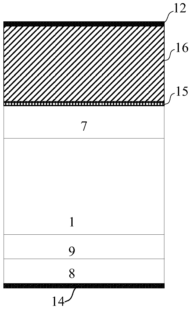
[0035] A plurality of deep grooves with the same structure deep into the voltage-resistant region 1 arranged on the upper surface of the semiconductor region, the deep grooves penetrate through the body contact region 5, the P-type base region 6 and the N-type carrier storage layer 3, and The N-type carrier storage layer 3 between the deep grooves is replaced by an N-type semiconductor r...

Embodiment 2

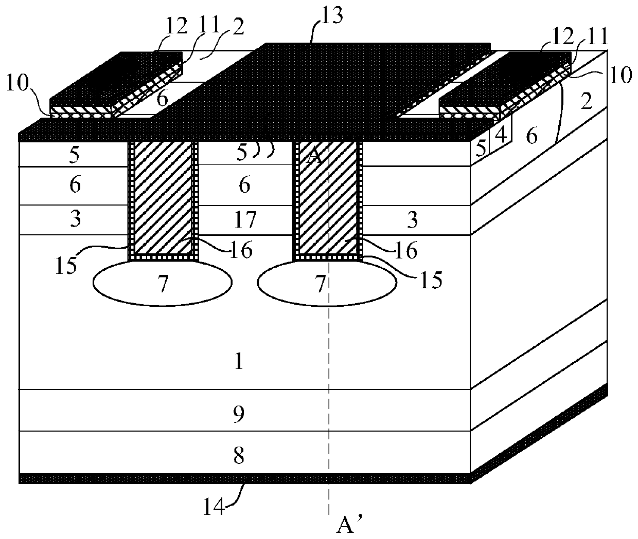
[0043] This embodiment provides a planar gate IGBT device with a carrier storage layer, the cell structure of which is as follows figure 2 As shown, the schematic diagram of the cut plane along AA' is as follows image 3 shown;

[0044] It differs from Embodiment 1 in that the direction of the channel current is parallel or approximately parallel to the sidewall of the deep trench.


PUM


Abstract

The invention relates to the field of power semiconductors, and provides a planar gate IGBT device with a deep trench electric field shielding structure, which is used for overcoming the problems thata current groove-gate IGBT gate with a carrier storage layer is too large in drive charges and small in short-circuit safety working region and is limited in the concentration of the CSL layer. The deep groove used for manufacturing the groove-gate IGBT channel traditionally and a P-type buried layer at the bottom portion of the groove are combined to form an electric field shielding structure toachieve clamping of the potential of the carrier storage layer; one IGBT cell is internally provided with a plurality of deep grooves to improve the concentration of the carrier storage layer of theIGBT compared to a traditional IGBT, have the higher cathode injection efficiency, and obtain the better trade-off relation of the on-state voltage and the turn-off loss. A planar gate and an electricfield shielding structure are employed, the IGBT has lower gate drive power consumption and lower saturation current density so as to improve the safety working region of the IGBT.

Description

technical field [0001] The invention relates to the field of power semiconductors, and specifically provides an IGBT device with low turn-on voltage drop, low driving power consumption and fast turn-off characteristics of a high short-circuit safe working area. Background technique [0002] IGBT compromises the low turn-on voltage drop of BJT and the fast switching characteristics of MOSFET, so it is widely used in power electronic systems. According to the structure of the IGBT gate, the IGBT can be divided into two types: the slot gate and the planar gate; the planar gate has low gate drive loss, and the saturation current density is low, and the short-circuit safe operating area is large, but due to the existence of the JEFT region, its The conduction voltage drop is large; the slot gate eliminates the JEFT area, so its conduction voltage drop is small, but due to the large channel density, its gate drive loss is large, and the saturation current density is high, thus sho...

Claims


Application Information

Patent Timeline
Patent Type & Authority Applications(China)
IPC IPC(8): H01L29/739H01L29/06H01L29/423
Inventor 易波李平
Owner UNIV OF ELECTRONICS SCI & TECH OF CHINA
Why Eureka
Try Eureka