A semiconductor device that takes into account the coordinated management of light and heat
A photothermal synergy and semiconductor technology, which is applied in semiconductor devices, electrical components, photovoltaic power generation, etc., can solve the problems of inability to realize photothermal synergy management and high transmittance, and achieve improved thermal radiation capability, low structural raw materials, Prepare simple effects
- Summary
- Abstract
- Description
- Claims
- Application Information
AI Technical Summary
Problems solved by technology
Method used
Image

Examples
Embodiment 1
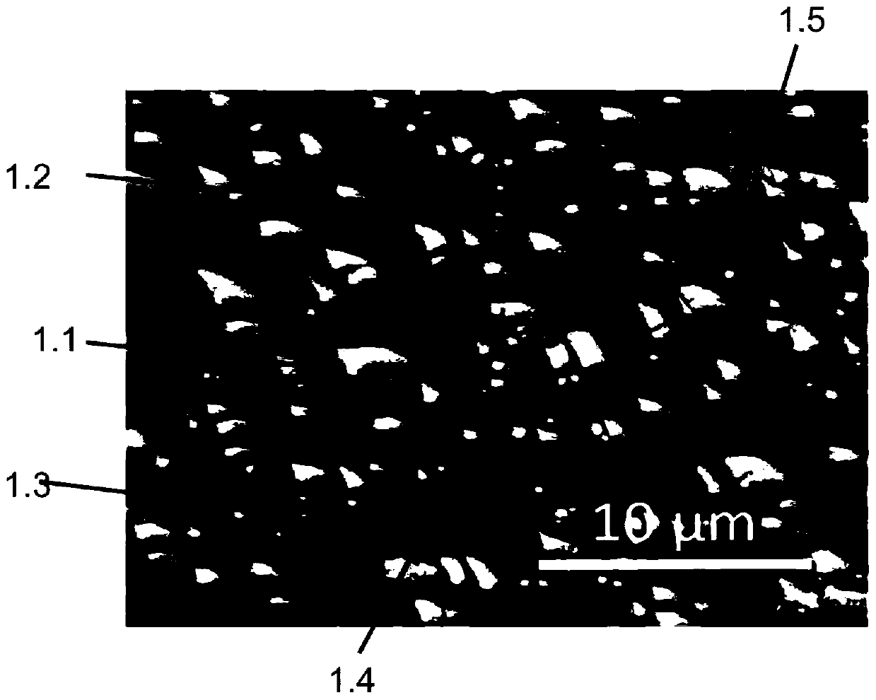
[0058] Select commercial textured silicon wafers, the textured characteristic size of which is 2-3um; mix polydimethylsiloxane and ethylenediamine at a mass ratio of 1:0.05; apply the polydimethylsiloxane mixture on The surface of the textured silicon wafer was cured at 40°C for 60 minutes; the cured polydimethylsiloxane micro-nano structure template was peeled off and set aside; commercial SiO with a solid content of 30% was selected 2 The sol is used as the initial sol; ethyl acetate butyl ether acetate is mixed with the initial sol at a mass ratio of 10% to obtain SiO 2 Sol;
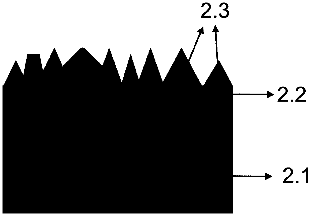
[0059] Such as figure 2 As shown, COB LED 2.1 is selected as the semiconductor optoelectronic device, cleaned with deionized water and dried; spin-coated SiO on the light-emitting surface 2.2 2 The sol is 5um thick and dry; use the polydimethylsiloxane micro-nano structure template prepared in this example, heat-cure and imprint at 100°C to transfer the pattern to the SiO on the light-emitting surf...
Embodiment 2
[0063] Select commercial textured silicon wafers, the textured characteristic size of which is 2-3um; mix polydimethylsiloxane, SYLGARD 184 silica gel, KH-570 silane at a mass ratio of 1:0.03:0.07, and polydimethylsiloxane The oxane mixture was coated on the surface of the textured silicon wafer, and cured at 60°C for 30 minutes; the cured polydimethylsiloxane micro-nano structure template was peeled off and set aside; commercial SiO with a solid content of 20% was selected 2 The sol is used as the initial sol; ethyl acetate butyl ether acetate is mixed with the initial sol at a mass ratio of 1% to obtain SiO 2 Sol;
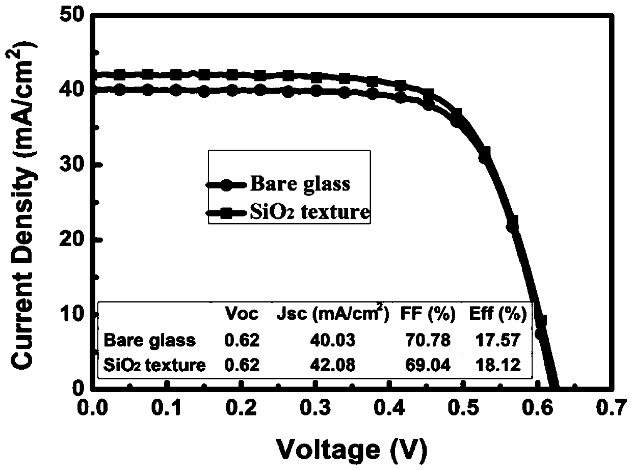
[0064] Select monocrystalline silicon cell components as semiconductor optoelectronic devices, wash with deionized water and dry; spin-coat SiO on the light incident glass 2 The sol is 2um thick and dry; transfer the pattern to the silica sol layer by using the aforementioned polydimethylsiloxane micro-nano structure template and 150°C heat-curing embossing, and...
Embodiment 3
[0067] Select the (100) surface single crystal silicon wafer; PECVD deposit 300nm silicon dioxide on the surface of the single crystal silicon as a protective layer; prepare a uniformly arranged photoresist array with a period of 3um and a side length of 2um on the silicon wafer through a photolithography process, And carry out post-baking and hardening film; prepare HF:NH 4 F: H 2 O=3:6:10 buffer HF solution; put the silicon wafer into the buffer HF solution and etch for 150s to obtain SiO with a side length of 2um, a period of 3um, and a uniform periodic arrangement 2 Masked (100) silicon wafers; put the silicon wafers into a 15% concentration of tetramethylammonium hydroxide (TMAH) solution, and corrode for 120 minutes at 70°C; obtain a micro-nano structure template with a period of 3um for later use;
[0068] Shop Commercial SiO 2 Nano sphere powder, SiO 2 The particle size of the nanosphere is 100nm~200nm; the SiO 2 Put the nano powder into the planetary grinder and g...
PUM
 Abstract
Description
Claims
Application Information
 - R&D
- Intellectual Property
- Life Sciences
- Materials
- Tech Scout
- Unparalleled Data Quality
- Higher Quality Content
- 60% Fewer Hallucinations
Browse by: Latest US Patents, China's latest patents, Technical Efficacy Thesaurus, Application Domain, Technology Topic, Popular Technical Reports.
© 2025 PatSnap. All rights reserved.Legal|Privacy policy|Modern Slavery Act Transparency Statement|Sitemap|About US| Contact US: help@patsnap.com