A radiation-resistant sense-switch type pflash switch unit structure and preparation method thereof

A switching unit, anti-radiation technology, applied in electrical components, semiconductor devices, circuits, etc., can solve problems such as narrowing of the erasing/writing threshold window, low programming time efficiency, floating gate charge loss, etc. Total Dose Radiation Capability, Reliability Enhancement Effect

Active Publication Date: 2021-05-25
58TH RES INST OF CETC
View PDF7 Cites 0 Cited by
  • Summary
  • Abstract
  • Description
  • Claims
  • Application Information

AI Technical Summary

Problems solved by technology

This structure is mainly based on the bulk silicon CMOS process integration, which has the advantages of simple process and high integration. However, the difficulty of the radiation-resistant hardening technology of the floating gate nFLASH basic unit lies in the total dose reinforcement, and its radiation damage by the total dose is mainly manifested as the erase / write threshold. Narrowing of the window, field edge leakage causes source-drain leakage and leakage between devices. The former causes electron emission in the programming state due to the total dose ionization effect, and the floating gate charge loss is caused by hole injection in the erasing state. The latter causes field leakage due to the total dose ionization effect. Region SiO 2 Trapped charges in the dielectric layer lead to a reduction in the inversion threshold voltage at the field edge of the p-substrate. At present, the anti-total dose radiation capability of this structure is about 50Krad(Si), which seriously limits its own anti-firmware error immunity, low power consumption, and reliability. The advantages of refactoring and other aspects are applied in the field of aerospace
Moreover, this structure mainly adopts the FN programming and FN erasing methods at present, and the selection of the programming method brings challenges to the high reliability of the device. time efficiency is also low

Method used


Image

  • A radiation-resistant sense-switch type pflash switch unit structure and preparation method thereof
  • A radiation-resistant sense-switch type pflash switch unit structure and preparation method thereof
  • A radiation-resistant sense-switch type pflash switch unit structure and preparation method thereof

Examples


Embodiment Construction

[0039]The present invention will be further described below in conjunction with specific drawings and examples.

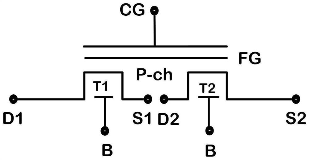
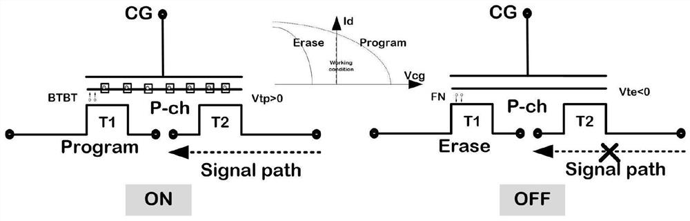
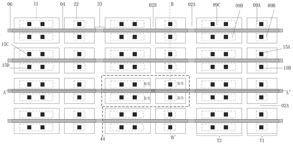
[0040]Such asFigure 7 withFigure 8As shown: in order to enhance the reliability and radiationability of the SENSE-SWITCH FLASH switch unit, the PFLASH switching unit 44 of the present invention includes a program / erase MOS tube T1 and a signal transmission MOS tube T2 on the same substrate 00 and a signal transmission MOS tube T2. The upper portion of the substrate 00 is provided with N well 01, the program / erase tube active region 22 of the program / erase MOS tube T1, the signal transmission tube active region 11 of the signal transmission MOS tube T2 is located in N Inside the well 01, the active zone isolation body 02b in the N well 01 is isolated;

[0041]The program / erase tube P + drain region 09a and the program / erase tube P + source region 09b are provided in the program / erase tube active region 22, and a signal transmission tube P + drain region is provided ...


PUM

PropertyMeasurementUnit
thicknessaaaaaaaaaa

Abstract

The invention relates to a radiation-resistant Sence-Switch type pFLASH switch unit structure and a preparation method thereof. The switching state of a programming / erasing tube to a signal transmission tube is realized by a floating gate charge sharing method, and the charge sharing method is BTBT programming and BTBT programming. FN erasing method; the radiation-resistant FLASH switch unit is fabricated in a silicon-based deep N well, and the signal transmission tube is effectively isolated from the active area of ​​the programming / erase tube through STI; the signal transmission tube gate oxide The layer and the programming / erase tube tunnel oxide layer are the same film layer, which is realized by N-doped oxidation process; the rest are made by industry standard process. The radiation-resistant Sence-Switch type pFLASH switch unit of the invention has a simple process, is compatible with the CMOS process, not only has good charge retention characteristics, durability, and a wide threshold window, but also has the advantages of strong anti-total dose capability and high programming efficiency. At the same time, the method for integrating the radiation-resistant Sence-Switch type pFLASH switch unit bulk silicon CMOS process of the present invention is also applicable to the SOI CMOS process.

Description

Technical field[0001]The present invention relates to a structure of a PFLASH switch unit and a preparation method thereof, in particular a radiation Sense-Switch type PFLASH switching unit structure and a preparation method thereof, specifically suitable for anti-radiation programmable logic devices (FPGA / CPLD) And the SENSE-SWITCH PFLASH switch unit structure of the SOC integrated circuit and the preparation method thereof, which belongs to the technical field of the microelectronic integrated circuit.Background technique[0002]Anti-radiation flash switching unit is a core basic composition unit that realizes the radiationable reconfigurable Flash-programmable logic device, compared to SRAM and anti-melt, and its performance is between the two, and its anti-radiation FLASH FPGA Process technology is the next-generation mainstream technology of anti-fuse FPGA process technology, and its military applications are mainly in the aerospace and aerospace sectors, including sea, land, e...

Claims


Application Information

Patent Timeline
Patent Type & Authority Patents(China)
IPC IPC(8): H01L27/11521H01L29/10H01L29/78
CPCH01L29/1079H01L29/7841H10B41/30
Inventor 刘国柱洪根深赵文斌曹利超朱少立
Owner 58TH RES INST OF CETC
Why Eureka
Try Eureka