High test density circuit test board

A technology of circuit testing and density, which is applied in the direction of electronic circuit testing, measuring electricity, measuring electrical variables, etc. It can solve the problems of destroying the probe structure, poor contact of the electrodes of the circuit board, and inaccessibility, so as to simplify the test steps and improve the measurement. Density, the effect of reducing the cost of testing

Active Publication Date: 2019-09-24
KINSUS INTERCONNECT TECH
View PDF5 Cites 0 Cited by
  • Summary
  • Abstract
  • Description
  • Claims
  • Application Information

AI Technical Summary

Problems solved by technology

[0010] It can be seen from the above description that the current circuit board testing device has the problem of insufficient test density. If the telescopic probe is tilted, it will be easy to wear, damage the structure of the probe, or cause poor contact with the electrodes of the circuit board due to insufficient length. In view of the problem of inaccessibility, the present invention provides a circuit test board with high test density to improve the above problems

Method used


Image

  • High test density circuit test board
  • High test density circuit test board
  • High test density circuit test board

Examples


Embodiment Construction

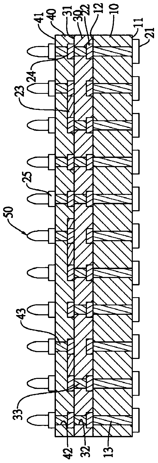
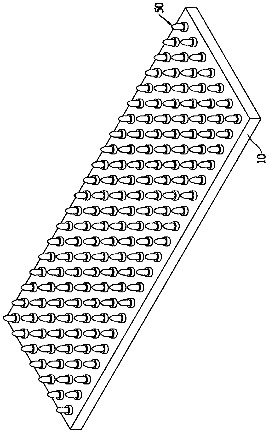
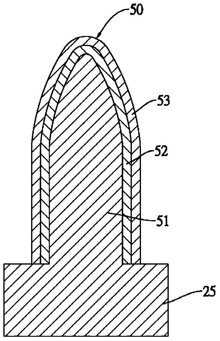
[0047] see figure 1 and figure 2 As shown, the present invention provides a circuit test board with high test density, comprising: a substrate 10, a plurality of lower electrodes 21, a plurality of upper electrodes 22, a first insulating layer 30, a wiring layer 23, a plurality of connection Electrodes 24 , a second insulating layer 40 , multiple surface electrodes 25 , and multiple conductive cones 50 .

[0048]The substrate 10 is a ceramic substrate. The substrate 10 has a lower surface 11 and an upper surface 12 opposite to the lower surface 11 .

[0049] The lower electrodes 21 are formed on the lower surface 11 of the substrate 10 , and the lower electrodes 21 are arranged in a matrix and arranged at intervals. These upper electrodes 22 are formed on the upper surface 12 of the substrate 10, and each upper electrode 22 is vertically corresponding to each lower electrode 21, wherein the substrate 10 is between the lower electrodes 21 and the upper electrodes 22 A plur...


PUM


Abstract

The invention provides a high test density circuit test board. The high test density circuit test board comprises a first substrate, a first insulation layer, a first wiring layer, a second insulation layer and a plurality of conductive cones; a plurality of lower electrodes and a plurality of upper electrodes are respectively arranged on a lower surface and an upper surface of the substrate; the lower electrodes are electrically connected to the upper electrodes; the first insulation layer is arranged on the upper surface of the substrate; the wiring layer is formed on the first insulation layer and the part of the upper electrodes are electrically connected through at least one first connector; the second insulation layer is arranged on the first insulation layer; and the conductive cones are formed on the second insulation layer in a matrix manner and is electrically connected to the wiring layer through at least one second connector. Through line arrangement of the wiring layer, the first connector and the second connector, electric test electric power is provided to part of the conductive cones and the electric test density is improved through the conductive cones.

Description

technical field [0001] The invention relates to a circuit test board, in particular to a circuit test board with high test density. Background technique [0002] The electrical test of the circuit board is one of the basic procedures for making the circuit board. It is used to check whether the circuit board can work smoothly. Therefore, it needs correct and complete tools to support it. In the electrical test, a circuit board is often stacked on a measurement On a test fixture of the device, the measuring device transmits power to the test fixture, and the test fixture selectively transmits power to electrodes or points to be tested on the circuit board to perform electrical testing on the circuit board. Please refer to Figure 5 As shown, the current test fixture 70 includes a bottom plate 71 , two spring elements 72 , a lift plate 73 , a plurality of telescopic probes 74 , and a mask plate 75 . The base plate 71 is formed with a plurality of concave holes 76, and the con...

Claims


Application Information

Patent Timeline
Patent Type & Authority Patents(China)
IPC IPC(8): G01R31/28G01R1/073
Inventor 林定皓张乔政林宜侬
Owner KINSUS INTERCONNECT TECH
Why Eureka
Try Eureka