Unlock instant, AI-driven research and patent intelligence for your innovation.

JTAG (Joint Test Action Group) interface multiplexing method and device

An interface multiplexing and interface technology, which is applied in the field of JTAG interface multiplexing methods and devices, can solve problems such as slow debugging speed, and achieve the effects of facilitating debugging analysis and improving access utilization.

Inactive Publication Date: 2017-10-27
HUNAN GOKE MICROELECTRONICS
View PDF10 Cites 2 Cited by
  • Summary
  • Abstract
  • Description
  • Claims
  • Application Information

AI Technical Summary

Problems solved by technology

[0005] This application provides a JTAG interface multiplexing method and device to solve the problem of slow debugging caused by JTAG interface multiplexing

Method used


Image

  • JTAG (Joint Test Action Group) interface multiplexing method and device
  • JTAG (Joint Test Action Group) interface multiplexing method and device
  • JTAG (Joint Test Action Group) interface multiplexing method and device

Examples


Embodiment Construction

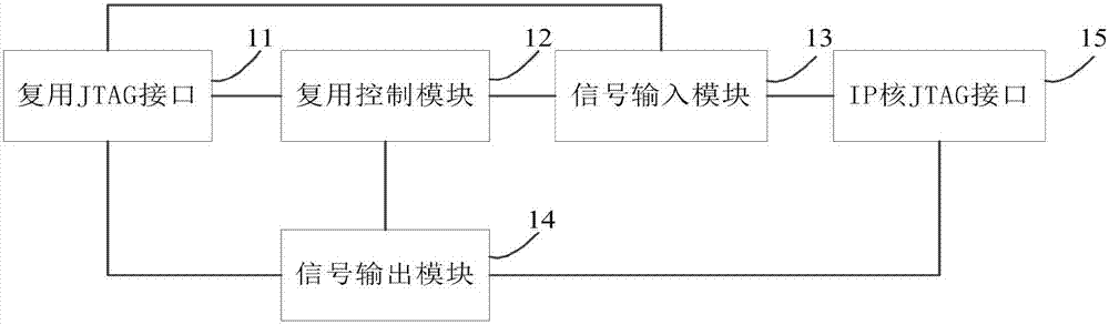
[0024] With the continuous improvement of the complexity and integration of ASIC (Application Specific Integrated Circuits) chips, there are a large number of IP (Intellectual Property) cores, most of which provide JTAG (Joint Test Action Group , Joint Test Working Group) interface, in order to save chip pins, multiple IP cores are required to multiplex a JTAG interface to facilitate the interconnection and multiplexing of the integrated JTAG controller interface. In order to solve the problem of slow debugging speed caused by JTAG interface multiplexing, the present application provides a JTAG interface multiplexing method and device.

[0025] see figure 1 , is a schematic structural diagram of a JTAG interface multiplexing device provided in the present application. see figure 2 , which is a structural schematic diagram of a signal input module provided by this application, see image 3 , is a schematic structural diagram of a signal output module provided in this applic...


PUM


Abstract

The invention discloses a JTAG (Joint Test Action Group) interface multiplexing method and device, relates to the technical field of integrated circuit testing, and is invited for solving the problem of low debugging speed caused by the JTAG interface multiplexing. The JTAG interface multiplexing device comprises a multiplexing control module, a signal input module and a signal output module, wherein the input end of the signal input module is connected with a multiplexed JTAG interface; the control end of the signal input module is connected with a multiplexing control module; the output end of the signal input module is connected with an IP (Internet Protocol) core JTAG interface; the input end of the signal output module is connected with the IP core JTAG interface; the control end of the signal output module is connected with the multiplexing control module; the output end of the signal output module is connected with the multiplexed JTAG interface; the input end of the multiplexing control module is connected with the multiplexed JTAG interface; and the output end of the multiplexing control module is independently connected with the control end of the signal input module and the control end of the signal output module. The method is mainly applied to a JTAG interface multiplexing process.

Description

technical field [0001] The present application relates to the technical field of integrated circuit testing, in particular to a JTAG interface multiplexing method and device. Background technique [0002] With the continuous improvement of the complexity and integration of ASIC (Application Specific Integrated Circuits) chips, there are a large number of IP (Intellectual Property, intellectual property) cores, and most of the IP cores provide JTAG (Joint Test Action Group (joint test working group) interface, in order to save chip pins, multiple IP cores are required to multiplex a JTAG interface to facilitate the interconnection and multiplexing of the integrated JTAG controller interface. [0003] In the prior art, the JTAG interface multiplexing mode is realized through the JTAG daisy chain, that is, to form a chain between the output terminals and the input terminals of multiple JTAG controllers, and the input terminals of the first-stage JTAG controllers are connected t...

Claims


Application Information

Patent Timeline
Patent Type & Authority Applications(China)
IPC IPC(8): G06F13/40
CPCG06F13/4022
Inventor 张国许建国姜黎彭鹏
Owner HUNAN GOKE MICROELECTRONICS
Features
  • R&D
  • Intellectual Property
  • Life Sciences
  • Materials
  • Tech Scout
  • Unparalleled Data Quality
  • Higher Quality Content
  • 60% Fewer Hallucinations
Learn More