Pixel compensating circuit, method, display driving device and display device

A compensation circuit and pixel technology, applied to static indicators, instruments, etc., can solve problems such as failure to turn off, negative shift of threshold voltage, flashing of light-emitting devices, etc., and achieve the effect of balancing the holding time and shortening the time

Active Publication Date: 2017-10-27
BOE TECH GRP CO LTD +1
View PDF8 Cites 10 Cited by
  • Summary
  • Abstract
  • Description
  • Claims
  • Application Information

AI Technical Summary

Problems solved by technology

Specifically, in the data writing phase T1, the first transistor TFT is controlled to be turned on by a high level, and the storage capacitor C st Charge to write the display data signal into the drive transistor; in the light-emitting stage, use the low level to control the first transistor TFT to turn off, and the storage capacitor C st Discharge, so that the drive transistor D is turned on, and the power signal drives the light emitting device L through the drive transistor D oled Lighting; drive the light-emitting device L through the 2T1C pixel compensation circuit oled The process of emitting light can be seen: the thin film transistor TFT is in the off state most of

Method used


Image

  • Pixel compensating circuit, method, display driving device and display device
  • Pixel compensating circuit, method, display driving device and display device
  • Pixel compensating circuit, method, display driving device and display device

Examples


Embodiment Construction

[0039] The following will clearly and completely describe the technical solutions in the embodiments of the present invention with reference to the accompanying drawings in the embodiments of the present invention. Obviously, the described embodiments are only some, not all, embodiments of the present invention. Based on the embodiments of the present invention, all other embodiments obtained by persons of ordinary skill in the art without creative efforts fall within the protection scope of the present invention.

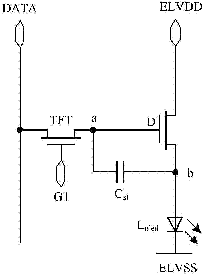
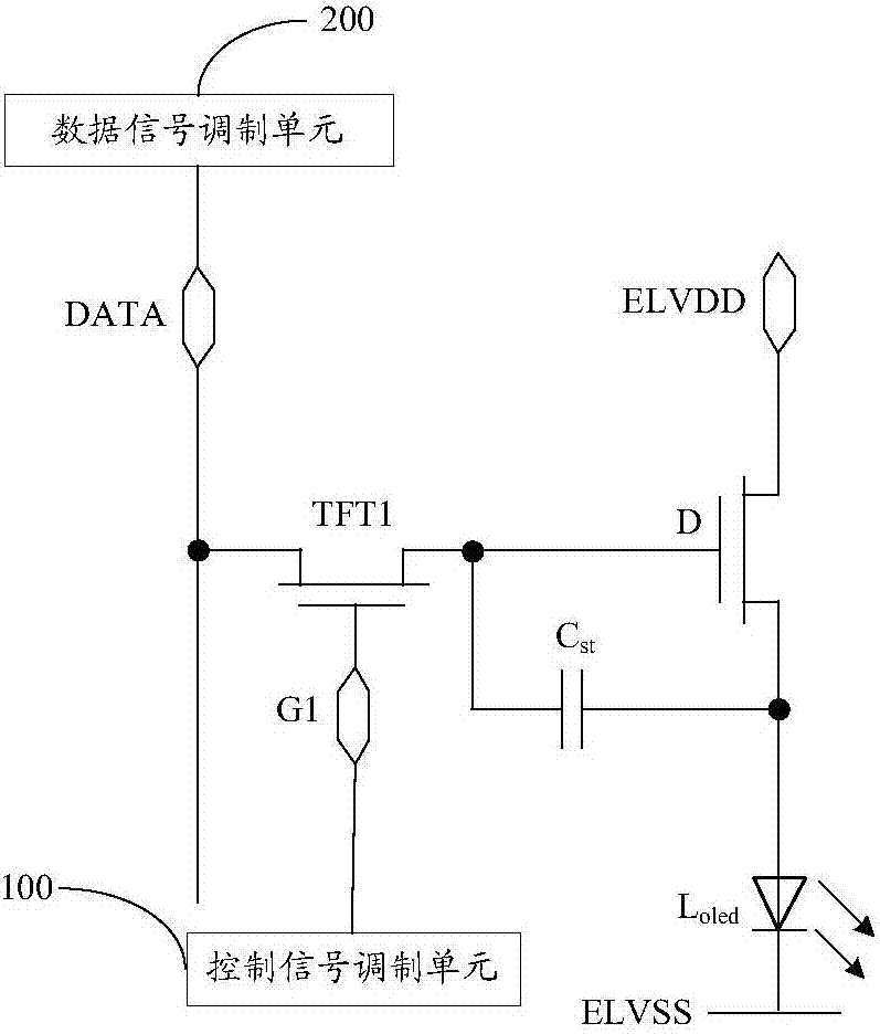
[0040] see image 3 , the pixel compensation circuit provided by the embodiment of the present invention includes: a first transistor TFT1, a driving transistor D and a storage capacitor C stThe control end of the first transistor TFT1 is connected to the control signal modulation unit 100, the input end of the first transistor TFT1 is connected to the data signal line, the output end of the first transistor TFT1 is connected to the control end of the driving trans...


PUM


Abstract

The invention discloses a pixel compensating circuit, a pixel compensating method, a display driving device and a display device, relates to the technical field of display, and aims to reduce the problems of a splash screen and empurpling of the display device caused by threshold voltage offset. The pixel compensating circuit comprises a first transistor; a control end of the first transistor is connected with a control signal modulation unit; an input end of the first transistor is connected with a data signal modulation unit; an output end of the first transistor is connected with a control end of a driving transistor; the output end of the first transistor is also connected with an output end of the driving transistor through a storage capacitor; an input end of the driving transistor is connected with a power signal line; the output end of the driving transistor is connected with a light emitting device; the control signal modulation unit and the data signal modulation unit modulate corresponding signals after a light emitting stage is ended, so that the grid source voltage direction at the time is opposite to the grid source voltage direction in the light emitting stage of the first transistor. The display driving device comprises the pixel compensating circuit. The pixel compensating circuit provided by the invention is used in an OLED (Organic Light-Emitting Diode) display device.

Description

technical field [0001] The present invention relates to the field of display technology, in particular to a pixel compensation circuit and method, a display driving device and a display device. Background technique [0002] Organic light-emitting diode (Organic Light-Emitting Diode, abbreviated as OLED) display device is a self-luminous display device, which is equipped with OLED devices arranged in an array, and controls the corresponding OLED devices to emit light through thin-film transistors to realize image display. . [0003] In the prior art, due to the instability of the film formation process, the threshold voltage of the thin film transistor has a certain deviation from the target threshold voltage. Therefore, a pixel compensation circuit is installed in the OLED display device to compensate the threshold voltage of the corresponding thin film transistor. . figure 1 A 2T1C pixel compensation circuit diagram is shown, which includes a thin film transistor TFT and ...

Claims


Application Information

Patent Timeline
IPC IPC(8): G09G3/3208
CPCG09G3/3208
Inventor 冯雪欢蔡振飞李永谦
Owner BOE TECH GRP CO LTD
Why Eureka
Try Eureka