Shift register unit, driving method thereof, display panel and display device

A technology for shifting register units and potentials, which is applied in information storage, static memory, static indicators, etc., and can solve problems such as circuit instability

Active Publication Date: 2017-11-03
WUHAN TIANMA MICRO ELECTRONICS CO LTD
View PDF5 Cites 2 Cited by
  • Summary
  • Abstract
  • Description
  • Claims
  • Application Information

AI Technical Summary

Problems solved by technology

[0004] Embodiments of the present invention provide a shift register unit, a driving method thereof, a disp

Method used


Image

  • Shift register unit, driving method thereof, display panel and display device
  • Shift register unit, driving method thereof, display panel and display device
  • Shift register unit, driving method thereof, display panel and display device

Examples


example 1

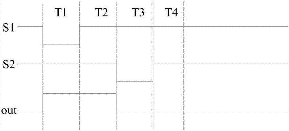
[0101] by image 3 Take the shift register unit shown as an example, all transistors in the shift register unit are P-type transistors, and the corresponding input and output timings are as follows: Figure 7 as shown, Figure 7 An input and output timing diagram corresponding to the shift register unit provided by the embodiment of the present invention; specifically, select such as Figure 7 The four stages T1, T2, T3 and T4 in the input timing diagram shown.

[0102] In the T1 stage, S1=0, S2=1, and S3=1.

[0103] Such as Figure 8a as shown, Figure 8a A schematic diagram of the working state of each transistor of the shift register unit in the T1 stage provided for the embodiment of the present invention; since S1=0, the first transistor M1 and the second transistor M2 are turned on. Since S3=1, the third transistor M3 is turned off. The high potential signal of the first signal terminal V1 is transmitted to the second node N2 through the second transistor M2, so th...

example 2

[0115] by Figure 5 Take the shift register unit shown as an example, all transistors in the shift register unit are N-type transistors, and the corresponding input and output timing is as follows Figure 9 as shown, Figure 9 Another input and output timing diagram corresponding to the shift register unit provided by the embodiment of the present invention; specifically, select such as Figure 9 The four stages T1, T2, T3 and T4 in the input timing diagram shown.

[0116] In the T1 stage, S1=1, S3=0.

[0117] Since S1=1, the first transistor M1 and the second transistor M2 are turned on. Since S3=0, the third transistor M3 is turned off. The low potential signal of the first signal terminal V1 is transmitted to the second node N2 through the second transistor M2, so the potential of the second node N2 is low, and the seventh transistor M7 is turned off. The high potential signal of the second signal terminal V2 is transmitted to the first node N1 through the first transi...


PUM


Abstract

The invention discloses a shift register unit, a driving method thereof, a display panel and a display device. The shift register unit comprises an output module, a first driver, a second driver, a first feedback regulation module and a second feedback regulation module, wherein the output module supplies a signal of a first signal end or a second signal end to an output end according to voltages exerted on a first node and a second node; the first driver controls the voltage of the first node according to a signal of a first input end; the second driver controls the voltage of the second node according to signals of the first input end and a third input end; the first feedback regulation module controls the voltage of the first node according to signals of the output end and a second input end; the second feedback regulation module controls the voltage of the second node according to the signal of the output end. The first feedback regulation module performs feedback control on the first node through the output end, and the second feedback regulation module can perform feedback control on the second node through the output end, so that in real-time positions of the first node and the second node, the circuit output is protected from external interference and the circuit reliability is improved.

Description

technical field [0001] The invention relates to the field of display technology, in particular to a shift register unit, a driving method thereof, a display panel and a display device. Background technique [0002] With the continuous development of display screens, consumers have higher and higher requirements for the stability of display screens. The stability of the display screen is largely reflected in the gate drive circuit and the shift register unit forming the gate drive circuit. [0003] At present, a shift register unit that uses scan signals as control signals such as Figure 1a as shown, Figure 1a A schematic structural diagram of a shift register unit provided for the prior art; including six transistors (M1-M6) and two capacitors (C1 and C2), wherein the first transistor M1 to the sixth transistor M6 are all P-type thin films transistor. Such as Figure 1b shown in the circuit timing diagram, Figure 1b for Figure 1a The circuit timing diagram correspond...

Claims


Application Information

Patent Timeline
IPC IPC(8): G11C19/28G09G3/20
CPCG09G3/20G09G2310/0286G11C19/28G09G5/003G09G2330/021G09G3/3677
Inventor 李玥朱仁远向东旭高娅娜陈泽源
Owner WUHAN TIANMA MICRO ELECTRONICS CO LTD
Why Eureka
Try Eureka