An FET type gas sensor having a composite insulating structure and a preparing method thereof

A gas sensor and composite insulation technology, which is applied in the direction of instruments, scientific instruments, measuring devices, etc., to achieve the effect of improving gas sensitivity characteristics, increasing sensitivity, and reducing the difficulty of device construction

Pending Publication Date: 2017-11-10
XINJIANG INST OF ENG
View PDF4 Cites 0 Cited by
  • Summary
  • Abstract
  • Description
  • Claims
  • Application Information

AI Technical Summary

Problems solved by technology

However, so far, there is no research report on the combination of two FET-type gas sensors to improve the sensitivity of FET-type gas sensors.

Method used


Image

  • An FET type gas sensor having a composite insulating structure and a preparing method thereof
  • An FET type gas sensor having a composite insulating structure and a preparing method thereof

Examples


Embodiment 1

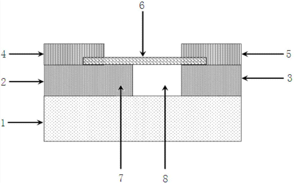
[0022] like figure 1 As shown, the FET type gas sensor with a composite insulating structure provided by the present invention includes a gate electrode 1, a first supporting layer 2, a second supporting layer 3, a source region 4, a drain region 5 and a micro-nano single crystal semiconductor 6 , wherein the width of the first support layer 2 is greater than the width of the source region 4 .

[0023] The first support layer 2 and the second support layer 3 are respectively fixed on both sides of the top of the gate electrode 1, the top of the first support layer 2 is glued and fixed to the source region 4, the first support layer 2 is not flush with the inner end of the source region 4, And the part inside the first support layer 2 that is longer than the source region 4 is a solid insulating layer 7 , and a first groove is opened inside the bottom of the source region 4 . The top of the second supporting layer 3 is glued and fixed to the drain region 5 , the second support...

Embodiment 2

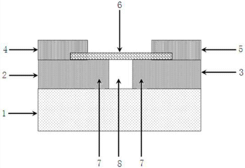
[0025] like figure 2 As shown, the structure of this embodiment is basically the same as that of Embodiment 1, the difference is that the width of the second support layer 3 in this embodiment is greater than the width of the drain region 5, and the second support layer 3 and the inner end of the drain region 5 The part inside the first support layer 2 that is longer than the source region 4 and the part inside the second support layer 3 that is longer than the drain region 5 are all solid insulating layers 7. The top of the gate electrode 1, the first support layer 2 and the second The gap between the supporting layers 3 and the cavity formed at the bottom of the micro-nano single crystal semiconductor 6 constitute an air-gap insulating layer 8 .

[0026] In the above embodiments, the gate electrode 1 can be a conductive substrate or an insulating substrate with a conductive material on top.

[0027] In each of the above-mentioned embodiments, the micro-nano single crystal ...


PUM

PropertyMeasurementUnit
diameteraaaaaaaaaa
thicknessaaaaaaaaaa

Abstract

The invention relates to an FET type gas sensor having a composite insulating structure and a preparing method thereof. The gas sensor and the method are characterized in that the gas sensor includes a gate electrode, first to second supporting layers, a source region, a drain electrode region and a micro-nano single crystal semiconductor; the top two sides of the gate electrode are provided with the first and second supporting layers; the top of the first supporting layer is adhered and fixed to the source region; the part in the first supporting layer, which is longer than the source region, is a solid insulation layer; the inside of the bottom of the source region is provided with a first groove; the top of the second supporting layer is adhered and fixed to the drain electrode region; the second supporting layer is flushed with the inner end part of the drain electrode region; the inside of the bottom of the drain electrode region is provided with a second groove; the micro-nano single crystal semiconductor is fixed at the tops of the first and second supporting layers; two ends of the micro-nano single crystal semiconductor are inserted into the first and second grooves respectively; a cavity formed by the gate electrode, the first supporting layer, the second supporting layer and the micro-nano single crystal semiconductor is an air gap insulating layer; and the gas sensor can be widely used in the field of gas sensors.

Description

technical field [0001] The invention relates to a FET type gas sensor with a composite insulating structure and a preparation method thereof, belonging to the field of gas sensors in the field of microelectronics. Background technique [0002] In the research and application of gas sensors, there are three basic parameters: sensitivity, selectivity and stability, which are usually called "3S" technology, and sensitivity is one of the most important parameters. First, high sensitivity is the guarantee of device reliability, anti-interference ability and other performances. Therefore, it is very important to improve the sensitivity of field effect transistor (FET) gas sensors in practical applications. [0003] In recent years, FET-type gas sensors have developed rapidly as another semiconductor gas-sensing device due to their advantages over resistive gas sensors. The characteristic of FET is that in addition to regulating the current with the source and drain regions, it ca...

Claims


Application Information

Patent Timeline
Patent Type & Authority Applications(China)
IPC IPC(8): G01N27/00
CPCG01N27/00
Inventor 塔力哈尔·夏依木拉提木拉里·马扎甫冯艳
Owner XINJIANG INST OF ENG
Why Eureka
Try Eureka