Electrophoresis display panel and manufacturing method thereof

An electrophoretic display and manufacturing method technology, applied in the direction of instruments, nonlinear optics, optics, etc., can solve the problems of reducing the capacitance of capacitor plates, failing to meet design requirements, and affecting the area of ​​capacitor plates, so as to increase capacitance, Meet display requirements and design flexible effects

Active Publication Date: 2017-11-10
SHANGHAI TIANMA MICRO ELECTRONICS CO LTD
View PDF7 Cites 6 Cited by
  • Summary
  • Abstract
  • Description
  • Claims
  • Application Information

AI Technical Summary

Problems solved by technology

[0005] However, since the scanning line 13, the metal replacement line 14 and the capacitor plate are arranged on the same film layer, this will affect the area of ​​the capacitor plate in the film layer, thereby reducing the electric charge between the two capacitor plates. capacity, which in turn cannot meet the design requirements during the hold phase

Method used


Image

  • Electrophoresis display panel and manufacturing method thereof
  • Electrophoresis display panel and manufacturing method thereof
  • Electrophoresis display panel and manufacturing method thereof

Examples


Embodiment Construction

[0030] The principles and features of the present application will be further described in detail below in conjunction with the drawings and embodiments. It should be understood that the specific embodiments described here are only used to explain related inventions, rather than to limit the invention. It should also be noted that, for ease of description, only parts related to the invention are shown in the drawings.

[0031] It should be noted that, in the case of no conflict, the embodiments in the present application and the features in the embodiments can be combined with each other. The present application will be described in detail below with reference to the accompanying drawings and embodiments.

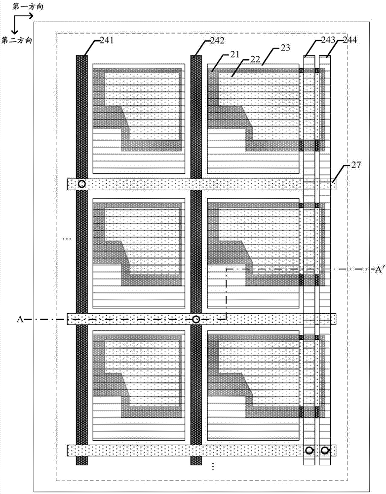
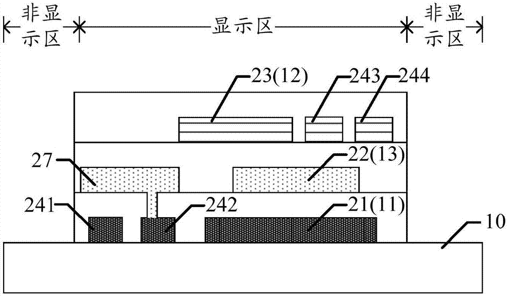
[0032] See figure 2 and image 3 , figure 2 A schematic structural view showing an embodiment of the electrophoretic display panel provided by the present application; image 3 yes figure 2 A cross-sectional structure diagram at A-A' of the electrophoretic display ...


PUM

PropertyMeasurementUnit
thicknessaaaaaaaaaa

Abstract

The embodiment of the application discloses an electrophoresis display panel and a manufacturing method of the electrophoresis display panel. The electrophoresis display panel comprises a substrate, a first metal layer located on the substrate, a second metal layer located on the first metal layer, a third metal layer located between the first metal layer and the second metal layer, and a plurality of metal change lines, wherein the substrate comprises a display area and a non-display area, a first capacitance plate is arranged on the first metal layer, a plurality of shading areas are arranged on the second metal layer, a second capacitance plate is arranged on the third metal layer, and the metal change lines extends along the section direction, are arranged along the first direction and are used for transmitting a data signal to a data line, wherein at least one of the metal change lines is located in the display area and is arranged on the second metal layer. Through adoption of the implementation mode, occupying the first metal layer and / or the third metal layer by the metal change line is reduced, so that the capacitance between the first capacitance plate and the second capacitance plate is increased to meet the display requirement.

Description

technical field [0001] The present application relates to the field of display technology, in particular to an electrophoretic display panel and a manufacturing method. Background technique [0002] At present, the basic principle of electrophoretic display is usually to control the moving position of electrophoretic particles through the electric field, and control the reflection of light through the moving position, so as to achieve the desired brightness. The structure of the existing electrophoretic display panel is generally to form an electrophoretic film between the pixel electrode and the common electrode. In this way, DC voltage signals are respectively provided to the pixel electrode and the common electrode, and an electric field can be formed between the two, thereby realizing picture display. The specific structure of the electrophoretic display surface can be found in figure 1 , which shows a schematic structural view of an existing electrophoretic display pa...

Claims


Application Information

Patent Timeline
Patent Type & Authority Applications(China)
IPC IPC(8): G02F1/167G02F1/1362G02F1/1333
CPCG02F1/1333G02F1/136286G02F1/167G02F1/136295
Inventor 许祖钊林柏全许文钦毛琼琴
Owner SHANGHAI TIANMA MICRO ELECTRONICS CO LTD
Why Eureka
Try Eureka