Ultra-thin ambient light and proximity sensor wafer level package and package method thereof

A technology of wafer-level packaging and proximity sensors, which is applied in the fields of electric solid-state devices, semiconductor devices, semiconductor/solid-state device manufacturing, etc., can solve the problems that restrict the development of thin sensors, the difficulty of thinning PCB substrates, and unfavorable miniaturization requirements. Achieve the effects of thinning design, increasing wiring density, and improving packaging accuracy

Pending Publication Date: 2016-10-12
宁波德葳智能科技有限公司
View PDF11 Cites 7 Cited by
  • Summary
  • Abstract
  • Description
  • Claims
  • Application Information

AI Technical Summary

Problems solved by technology

Ambient light and proximity sensors combine a light-sensing chip and a light-emitting chip. Traditionally, the two chips are manufactured using different wafers, and then assembled on a PCB substrate for packaging; because the PCB substrate is difficult to thin, this kind of sensor is restricted. thin development
[0003] Wire bonding or wire bonding (Wire Bonding) is used to connect the PCB substrate, the photosensitive chip and the light emitting chip. It needs to be operated one by one, and the production efficiency is low, which leads to high cost and is not conducive to miniaturization requirements.

Method used


Image

  • Ultra-thin ambient light and proximity sensor wafer level package and package method thereof
  • Ultra-thin ambient light and proximity sensor wafer level package and package method thereof
  • Ultra-thin ambient light and proximity sensor wafer level package and package method thereof

Examples


Embodiment Construction

[0039] In order to make the above objects, features and advantages of the present invention more comprehensible, examples will be given below to illustrate the specific implementation of the present invention in detail. The specific embodiments of the present invention are set forth in the following description to fully understand the present invention. However, the present invention can be implemented in a manner different from the following description, and those skilled in the art can make similar extensions without departing from the connotation of the present invention. Accordingly, the present invention is not limited to the specific Examples disclosed below.

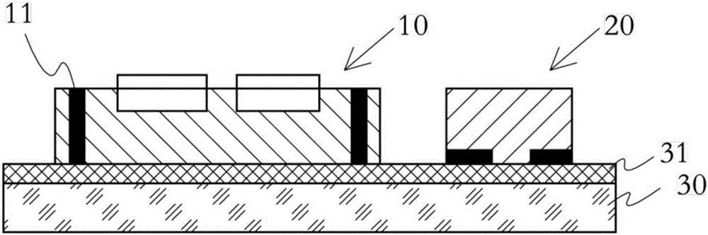
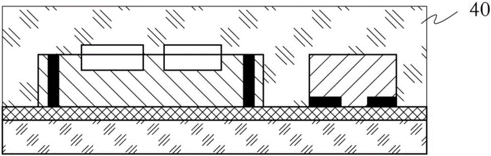
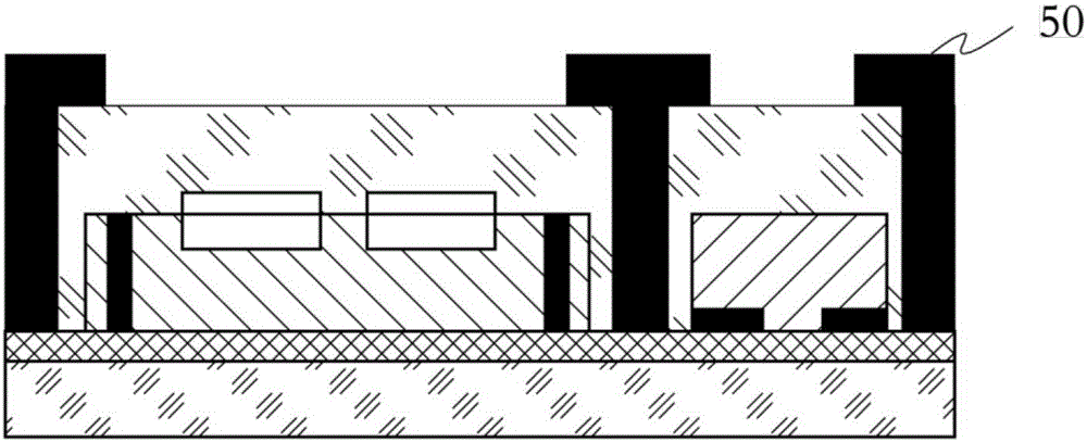
[0040] The wafer-level packaging method of the ultra-thin ambient light and proximity sensor in this embodiment is as follows: Figure 1 to Figure 5 shown.

[0041] First, prepare a photosensitive wafer 10 with TSVs 11. The photosensitive wafer 10 can be an ambient light sensor (Ambient Light Sensor), or a proxim...


PUM


Abstract

The invention provides ultra-thin ambient light and proximity sensor wafer level package and a package method thereof. The method comprises the steps that a. a light-sensitive wafer with a silicon through-hole structure and a light-emitting wafer are placed on a forming carrier with a tape; b. the light-emitting wafer and the light-sensitive wafer are encapsulated by a light-transmitting material to form an optical cover; c. the optical cover is encapsulated by a non-light-transmitting material, and a light isolation belt is formed between the light-emitting wafer and the light-sensitive wafer to form a protection cover; d. the top of the protection cover is bonded to the processing fixture of an RDL wiring layer; e. the forming carrier and the tape are removed; and f. the RDL wiring layer is formed on the removed surface to realize the wafer level package. According to the invention, traditionally relying on the process of a PCB substrate is changed; the light-sensitive wafer with the silicon through-hole structure and the RDL wiring layer are combined to realize wafer level package; and thinning and efficient production are realized without the PCB substrate.

Description

technical field [0001] The invention relates to sensor packaging technology, in particular to a wafer-level packaging of an ultra-thin ambient light and proximity sensor and a packaging method thereof. Background technique [0002] The miniaturization of smart devices is based on the miniaturization of their components. Ambient light and proximity sensors combine a light-sensing chip and a light-emitting chip. Traditionally, the two chips are manufactured using different wafers, and then combined on the PCB substrate for packaging; the PCB substrate is difficult to thin, which restricts this sensor. thin development. [0003] The PCB substrate, the light sensing chip and the light emitting chip are connected by wire bonding or wire bonding (Wire Bonding), which needs to be operated one by one, and the production efficiency is low, which leads to high cost and is not conducive to miniaturization requirements. Contents of the invention [0004] As mentioned above, how to b...

Claims


Application Information

Patent Timeline
Patent Type & Authority Applications(China)
IPC IPC(8): H01L21/56H01L25/16H01L23/48
CPCH01L24/02H01L25/167H01L21/568H01L23/481H01L2224/0231H01L2224/02372H01L2224/04105H01L2224/12105H01L2224/19
Inventor 张珊珊林挺宇林海斌蔡旭
Owner 宁波德葳智能科技有限公司
Why Eureka
Try Eureka