Multilayer flexible circuit board manufacturing method

A flexible circuit board and manufacturing method technology, which is applied in multilayer circuit manufacturing, printed circuit manufacturing, printed circuit and other directions, can solve the problems of long manufacturing process, difficulty in inter-layer alignment, and long production time, so as to reduce process steps and save money. The effect of process time

Active Publication Date: 2020-02-28
AVARY HLDG (SHENZHEN) CO LTD +2
View PDF5 Cites 0 Cited by
  • Summary
  • Abstract
  • Description
  • Claims
  • Application Information

AI Technical Summary

Problems solved by technology

[0003] The existing multi-layer flexible circuit boards mostly use the method of gradually adding layers and forming holes in a single layer to form plated holes to electrically connect two adjacent conductive layers. However, this method is not only difficult to align between layers, but also The production process is longer and the production time is longer
The existing multi-layer flexible circuit board also has a through hole penetrating through the upper and lower sides of the insulating substrate directly on the substrate, and a columnar metal needle is riveted in the through hole, and the metal needle is electrically connected to the conductive layer above and below the insulating substrate. However, the multilayer flexible circuit board made by this method cannot realize the electrical connection between any two conductive layers.

Method used


Image

  • Multilayer flexible circuit board manufacturing method
  • Multilayer flexible circuit board manufacturing method
  • Multilayer flexible circuit board manufacturing method

Examples


Embodiment Construction

[0090] The following will be combined with Figure 1-19 and two embodiments, the multi-layer flexible circuit board provided by the technical solution and its manufacturing method are further described in detail.

[0091] Please refer to Figure 1-9 , the manufacturing method of the multilayer flexible circuit board 100a of the first embodiment of the present invention, it comprises the following steps:

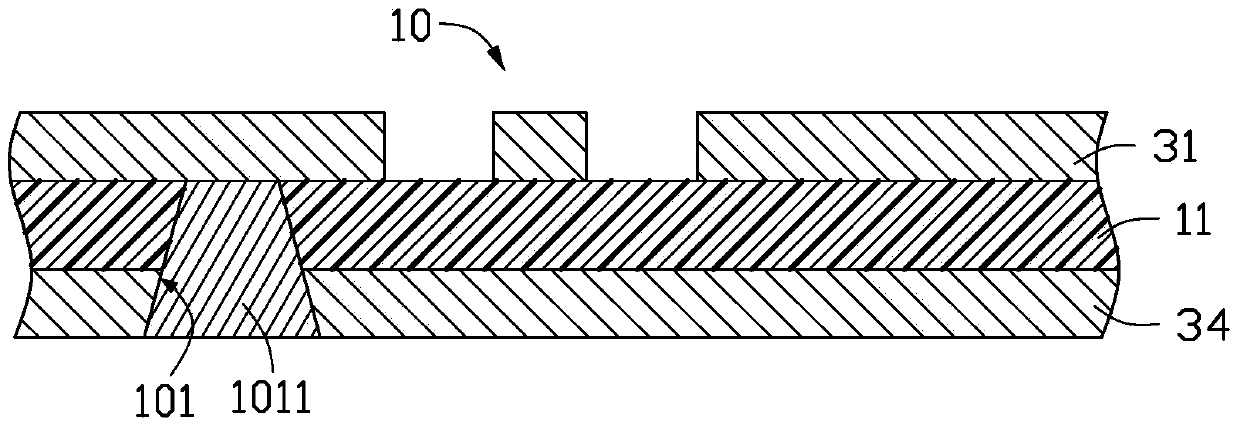
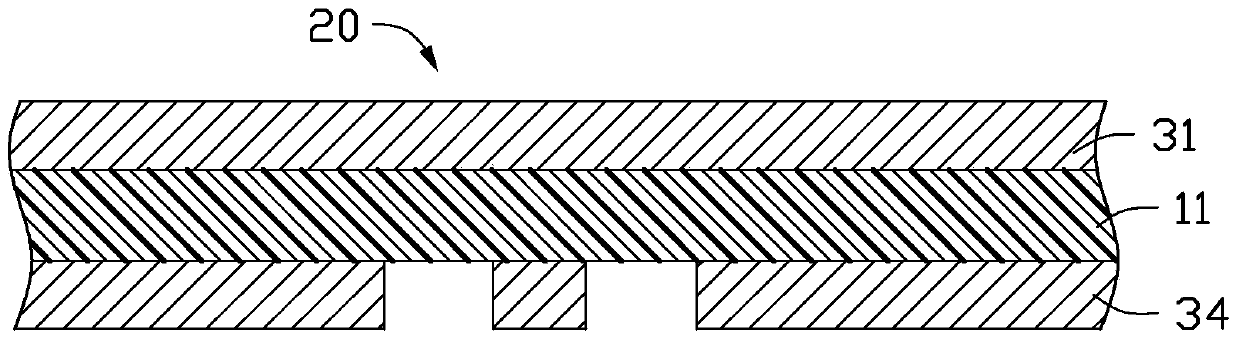
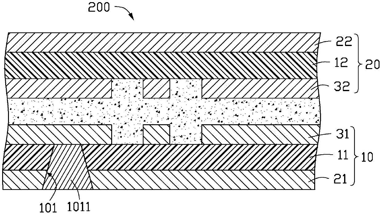
[0092] Step S1: See figure 1 , providing a first double-sided copper-clad laminate 10, the first double-sided copper-clad laminate 10 includes a first insulating layer 11, a first copper layer 21 bonded to a surface of the first insulating layer 11, and a first copper layer 21 bonded to the first The first inner conductive circuit layer 31 on the surface of the insulating layer 11 away from the first copper layer 21 . The first double-sided copper clad board 10 is provided with a first first-order blind hole 101, the opening of the first first-order blind hole 101 is opene...


PUM


Abstract

A multi-layer flexible circuit board comprises a plurality of conductive circuit layers and a plurality of insulation layers, wherein the insulation layer is arranged between adjacent conductive circuit layers, a plurality of first-order blind holes and a plurality of second-order blind holes are formed in the multi-layer flexible circuit board, the first-order blind holes are filled with first-order conductive posts, the second-order blind holes are filled with second-order conductive posts, the first-order conductive posts and the second-order conductive posts are matched to make the plurality of conductive circuit layers electrically connected, the plurality of conductive circuit layers comprise a first external conductive circuit layer, a second external conductive circuit layer and a plurality of internal conductive circuit layers, the plurality of second-order blind holes comprise a first second-order blind hole, the first second-order blind hole is filled with a first second-order conductive post, the plurality of internal conductive circuit layers comprise a first internal conductive circuit layer, a second internal conductive circuit layer and a third internal conductive circuit layer which are adjacent to one another, and the first internal conductive circuit layer, the second internal conductive circuit layer and the third internal conductive circuit layer are electrically connected by the first second-order conductive post. Moreover, the invention also provides a fabrication method of the multi-layer flexible circuit board.

Description

technical field [0001] The invention relates to a method for manufacturing a multilayer flexible circuit board. Background technique [0002] Flexible printed circuit boards (Flexible Printed Circuit Board, FPC) have the advantages of bendability, light weight, small footprint, and three-dimensional wiring. They are used in notebook computers, liquid crystal displays, digital cameras, mobile phones, digital cameras, smart watches, etc It has a very wide range of applications in consumer electronics. With the improvement of people's requirements for processing information of consumer electronics products, because the multilayer circuit board has multilayer circuit layers and thus has more wiring area, the flexible multilayer circuit board gradually replaces the flexible single-sided circuit board and flexible double-sided circuit board. Surface circuit boards are increasingly used in consumer electronics. Multilayer flexible circuit boards in wearable products are increasin...

Claims


Application Information

Patent Timeline
Patent Type & Authority Patents(China)
IPC IPC(8): H05K3/46
CPCH05K3/4614H05K3/4635H05K2201/058
Inventor 李艳禄姚青春何明展
Owner AVARY HLDG (SHENZHEN) CO LTD
Why Eureka
Try Eureka