Impedance test method based on de-embedding

An impedance test and de-embedding technology, applied in the field of testing, can solve the problems of long cycle time, high price, and decreased design efficiency of chip test probes, and achieve the effect of avoiding test limitations, reducing costs, and reducing cycles.

Active Publication Date: 2017-11-14
SHANGHAI IC TECH & IND PROMOTION CENT
View PDF8 Cites 6 Cited by
  • Summary
  • Abstract
  • Description
  • Claims
  • Application Information

AI Technical Summary

Problems solved by technology

At present, there are also special units to design corresponding RF probe fixtures to test chip parameters. References (1. A calibration method for the S-parameter amplitude-frequency characteristics of modular probes; There are their own methods, but these test RF probes have the limitation of the distance of the chip test PAD. In addition, the cycle of equipped with chip test probes is relatively long and the price is relatively expensive, which results in an increase in the production design cycle and cost. Efficiency drops

Method used


Image

  • Impedance test method based on de-embedding
  • Impedance test method based on de-embedding
  • Impedance test method based on de-embedding

Examples


Embodiment Construction

[0032] The embodiments of the present invention will be described in detail below in conjunction with the accompanying drawings, but the present invention can be implemented in many different ways defined and covered by the claims.

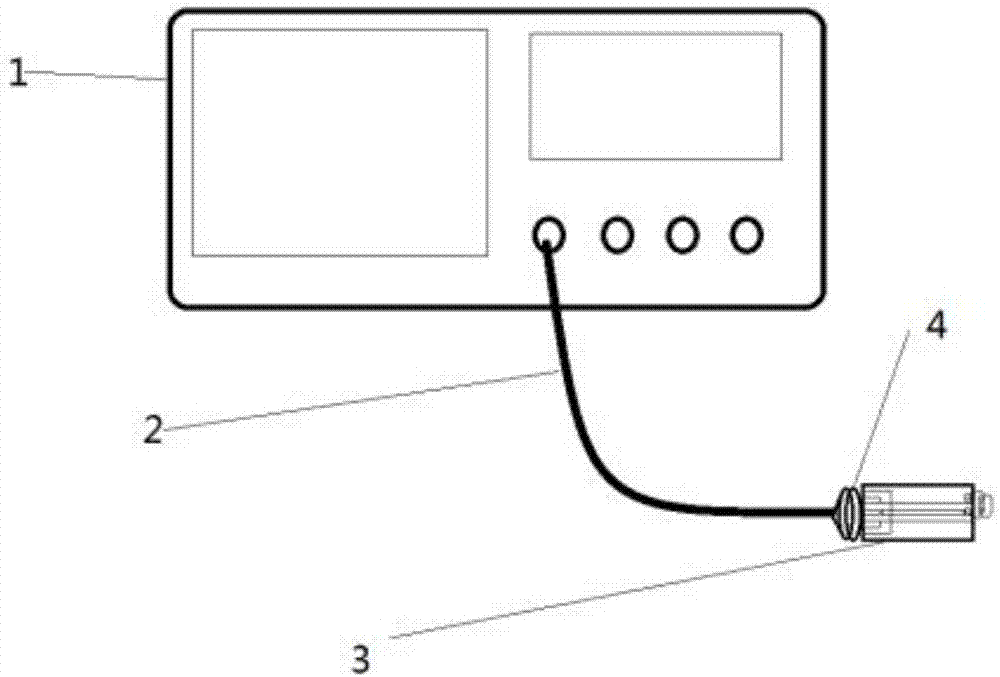
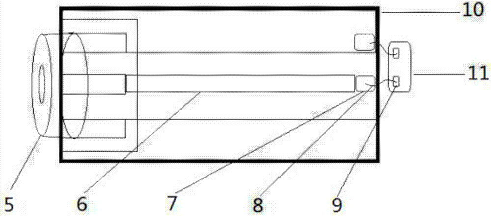
[0033] Such as Figure 1-9 As shown, among them, 1-vector network analyzer, 2-transmission cable, 3-tested sample, 4-cable conversion interface, 5-SMA adapter A, 6-video transmission line, 7-PCB binding PAD, 8-chip bonding wire, 9-the tested chip is bound to the PAD, 10-PAB test circuit board, 11-the chip to be tested, 12-SMA adapter B, 13-microstrip lines of different lengths.

[0034] An impedance testing method in a de-embedding manner, comprising the following steps:

[0035] (1) Hardware preparation:

[0036] PCB board for bonding required for testing;

[0037] (2) Consistency measurement:

[0038] Measure the COB of the bonded chip, record and compare its S11 file, and observe its consistency; according to the label sensitivity provided ...


PUM


Abstract

The invention discloses an impedance test method based on de-embedding, including the following steps: (1) hardware preparation; (2) consistency measurement; (3) determining a micro-strip line de-embedding board; (4) determining a chip mounting capacitor; (5) determining a final impedance test de-embedding board; and (6) measurement. The impedance test method based on de-embedding replaces the original long-cycle and expensive chip impedance test method using a high-frequency probe. The cycle of the S parameter method provided by the invention is about three days. The cycle of radio-frequency chip impedance test is shortened greatly. The test method of the invention avoids the test limitation caused by fixed spacing between radio-frequency probe tips, and reduces the cost of impedance test.

Description

technical field [0001] The invention relates to a detection method, in particular to a de-embedding impedance testing method. Background technique [0002] With the advancement of semiconductor technology and the rapid development of the information industry, RF / microwave semiconductor devices are used more and more widely, so more and more attention is paid to the measurement of device parameters during design. Not only chip designers need to know how to accurately measure chip parameters, chip users also hope to get more accurate parameters. In the S-parameter measurement of microwave network, the measurement of chip parameters will inevitably encounter measurement errors caused by chip bonding lines and transmission lines. At present, there are also special units that design corresponding RF probe fixtures to test chip parameters. References (1. A calibration method for the S-parameter amplitude-frequency characteristics of modular probes; There are their own methods, b...

Claims


Application Information

Patent Timeline
IPC IPC(8): G01R27/02G01R27/28G01R31/28
CPCG01R27/02G01R27/28G01R31/2822
Inventor 姜祁峰丁立业朱小炜
Owner SHANGHAI IC TECH & IND PROMOTION CENT
Why Eureka
Try Eureka