Substrate cleaning method and film forming method

A film-forming method and substrate technology, which is applied in the fields of electrical components, semiconductor/solid-state device manufacturing, circuits, etc., can solve the problems of substrate dropping oil stains, water marks and foreign objects, and affecting yield, so as to improve cleanliness and achieve cleanliness , Improve the effect of film forming quality

Active Publication Date: 2017-11-14
WUHAN CHINA STAR OPTOELECTRONICS TECH CO LTD
View PDF3 Cites 5 Cited by
  • Summary
  • Abstract
  • Description
  • Claims
  • Application Information

AI Technical Summary

Problems solved by technology

[0013] 1. Water mark problem: The substrate passes through many wet units before film formation. If the final drying process is not sufficient, moisture will remain on the substrate, and water marks and foreign objects will be formed after film formation, which will affect the yield rate;
[0014] 2. Oil pollution problem: the substrate is transported through a long path before film formation, and it is easy to drop oil stains on the substrate, and it is easy to cause wrinkles after film formation, which will also affect the yield

Method used


Image

  • Substrate cleaning method and film forming method
  • Substrate cleaning method and film forming method
  • Substrate cleaning method and film forming method

Examples


Embodiment Construction

[0038] In order to further illustrate the technical means and effects adopted by the present invention, the following describes in detail in conjunction with the embodiments of the present invention and the accompanying drawings.

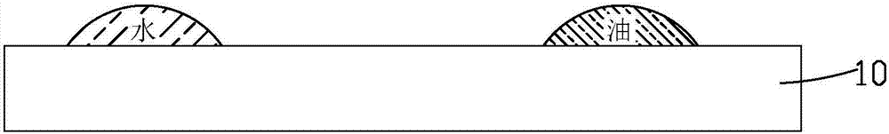
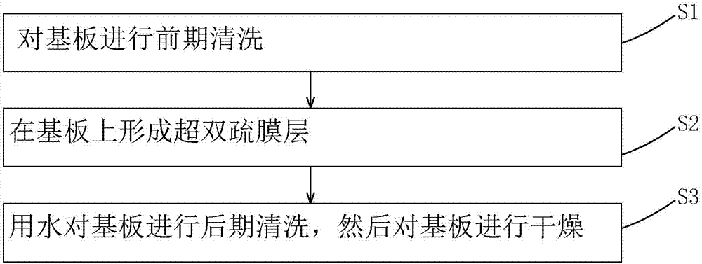
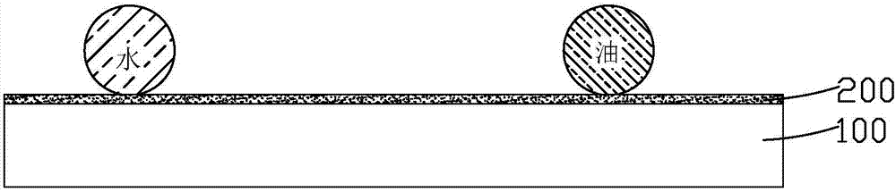
[0039] see figure 2 , a kind of substrate cleaning method that the present invention firstly provides, comprises the following steps:

[0040] Step S1 , pre-cleaning the substrate 100 .

[0041] Specifically, the process of pre-cleaning the substrate 100 in step S1 of the present invention may include the following steps S11 to S14 in sequence according to the specific conditions of the substrate 100, and may also optionally include the following steps; The substrate 100 described in the embodiment is used to form a low temperature polysilicon (Low Temperature Poly-silicon, LTPS) TFT substrate, the upper surface of the substrate 100 is the surface of the amorphous silicon layer, and the substrate 100 is cleaned in the early stage in the step S1 T...


PUM


Abstract

The invention provides a substrate cleaning method and a film forming method. The substrate cleaning method provided by the invention comprises the steps that a substrate is pre-cleaned; a super-amphiphobic film layer is formed on the substrate; and finally, the substrate is washed with water in the latter stage. The lyophobic and oleophobic super-amphiphobic film layer is formed on the pre-cleaned substrate to avoid the problems of subsequent water marks and oil pollution. The cleanliness of the substrate before film forming is improved. The film forming quality can be effectively improved. The product yield is improved. The electrical properties of the substrate are not impacted. According to the film forming method provided by the invention, the substrate cleaning method is used to clean the substrate before film forming; the cleanliness of the substrate before film forming is improved; the film forming quality can be effectively improved; the product yield is improved; and the electrical properties of the substrate are not impacted.

Description

technical field [0001] The invention relates to the technical field of display panel manufacturing, in particular to a substrate cleaning method and a film forming method. Background technique [0002] In the field of display technology, flat-panel displays such as Liquid Crystal Display (LCD) and Organic Light Emitting Diode (OLED) have gradually replaced CRT displays, and are widely used in LCD TVs, mobile phones, personal digital assistants, digital Cameras, computer or laptop screens, etc. [0003] The display panel is an important part of LCD and OLED. Whether it is an LCD display panel or an OLED display panel, it usually has a thin film transistor (Thin Film Transistor, TFT) array substrate. Taking the LCD display panel as an example, it is mainly composed of a TFT array substrate, a color filter substrate (Color Filter, CF), and a liquid crystal layer (Liquid Crystal Layer) arranged between the two substrates. Its working principle The rotation of the liquid cryst...

Claims


Application Information

Patent Timeline
Patent Type & Authority Applications(China)
IPC IPC(8): H01L21/02
CPCH01L21/02057
Inventor 卢瑞
Owner WUHAN CHINA STAR OPTOELECTRONICS TECH CO LTD
Why Eureka
Try Eureka