Substrate cleaning equipment and substrate cleaning method

A technology for cleaning equipment and substrates, which is applied in semiconductor devices, electrical components, circuits, etc., and can solve the problems of large electrical influence of thin film transistors

Pending Publication Date: 2021-03-02
SHENZHEN CHINA STAR OPTOELECTRONICS SEMICON DISPLAY TECH CO LTD
View PDF4 Cites 0 Cited by
  • Summary
  • Abstract
  • Description
  • Claims
  • Application Information

AI Technical Summary

Problems solved by technology

However, ultraviolet light has a greater impact on the electrical ...

Method used


Image

  • Substrate cleaning equipment and substrate cleaning method
  • Substrate cleaning equipment and substrate cleaning method
  • Substrate cleaning equipment and substrate cleaning method

Examples


Embodiment Construction

[0034] The technical solutions in the embodiments of the present application will be clearly and completely described below in conjunction with the drawings in the embodiments of the present application. Apparently, the described embodiments are only some of the embodiments of this application, not all of them. Based on the embodiments in this application, all other embodiments obtained by those skilled in the art without making creative efforts belong to the scope of protection of this application.

[0035] Embodiments of the present application provide a substrate cleaning device and a substrate cleaning method, which will be described in detail below.

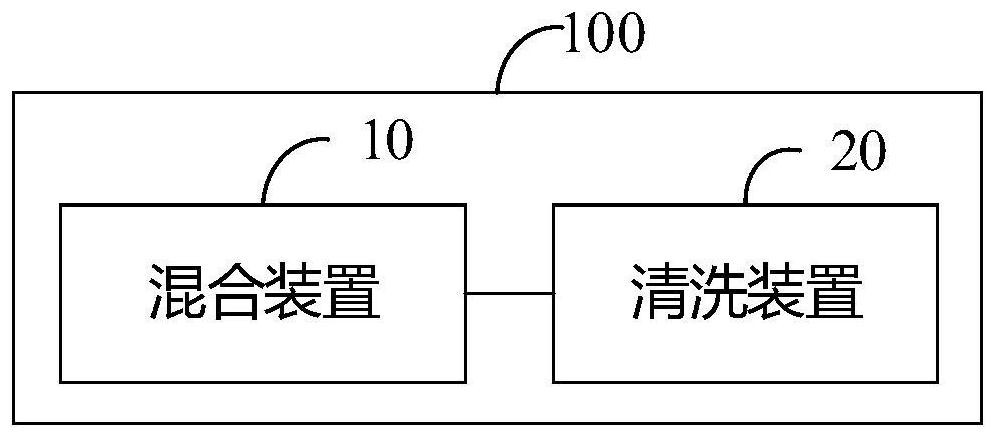
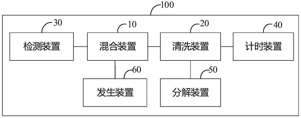
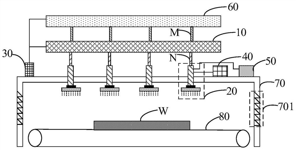
[0036] see figure 1 , figure 1 It is a schematic structural diagram of the substrate cleaning equipment provided in the embodiment of the present application. The substrate cleaning device 100 includes a mixing device 10 and a cleaning device 20 . Wherein, the mixing device 10 is used for mixing ozone and water to form o...


PUM


Abstract

The embodiment of the invention provides substrate cleaning equipment and a substrate cleaning method. The substrate cleaning equipment comprises a mixing device and a cleaning device. The mixing device is used for mixing ozone and water to form ozone water; and the cleaning device is used for cleaning the substrate by utilizing the ozone water formed in the mixing device. According to the scheme,the ozone is dissolved in the water, and the substrate is cleaned by utilizing the ozone water, so that the influence of ultraviolet light on the electrical property of a thin film transistor on thesubstrate can be avoided.

Description

technical field [0001] The present application relates to the field of display technology, in particular to a substrate cleaning device and a substrate cleaning method. Background technique [0002] In the fabrication of organic light-emitting diode (Organic Light-Emitting Diode, OLED) devices, energy level matching is a very important device design principle. The core of energy level matching lies in the control of hole carriers. Generally, the work function of the anode and the hole injection ability are enhanced by surface treatment of the anode. The common method of surface treatment of the anode is ultraviolet light treatment. [0003] The main principle of using ultraviolet light to treat the substrate is that under the action of ultraviolet light, oxygen is converted into ozone. Ozone has strong oxidizing properties, can remove dirt on the surface of the substrate, and can partially improve the work function of the anode. However, ultraviolet light has a greater infl...

Claims


Application Information

Patent Timeline
IPC IPC(8): H01L21/67H01L51/56H01L27/32
CPCH01L21/67023H10K59/00H10K71/00
Inventor 李祥龙
Owner SHENZHEN CHINA STAR OPTOELECTRONICS SEMICON DISPLAY TECH CO LTD
Why Eureka
Try Eureka