Forming method of memory device
A memory and wet etching technology, applied in the direction of electric solid state devices, semiconductor devices, electrical components, etc.
- Summary
- Abstract
- Description
- Claims
- Application Information
AI Technical Summary
Problems solved by technology
Method used
Image
Examples
Embodiment Construction
[0033] The following describes the present disclosure more fully with reference to the drawings of the embodiments of the present disclosure. However, the present disclosure can also be embodied in various forms, and should not be limited to the embodiments described herein. The thicknesses of layers and regions in the drawings may be exaggerated for clarity. The same or similar reference numerals denote the same or similar elements, and the following paragraphs will not repeat them one by one.
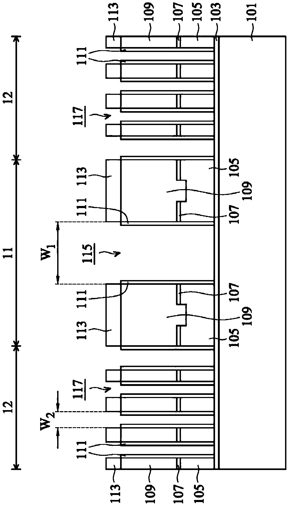
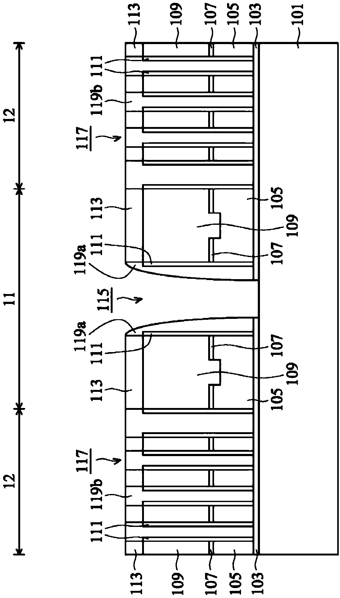
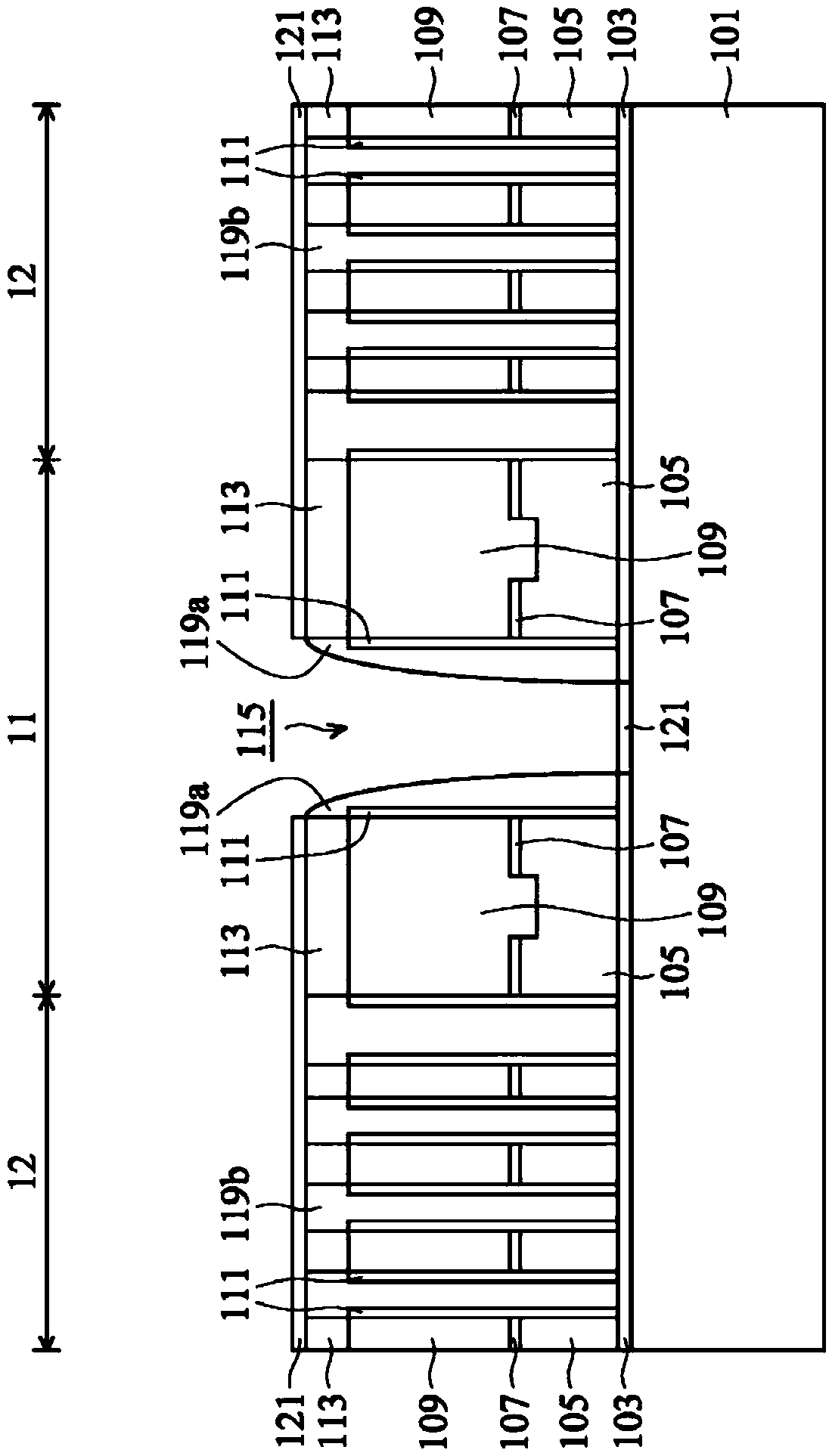
[0034] Figure 1-Figure 9 is according to some embodiments of the present disclosure, showing the formation of Figure 9 A schematic cross-sectional view of different stages of the memory device 100 .
[0035] like figure 1 As shown, a substrate 101 is provided, and the substrate 101 includes a peripheral circuit area 11 and an array area 12 adjacent to the peripheral circuit area 11 . In some embodiments, the material of the substrate 101 may include silicon, gallium arsenide, g...
PUM
 Abstract
Description
Claims
Application Information


