
Method and structure for impriving the measurment accuracy of LDD doping layer square resistance

A technology for sheet resistance and measurement accuracy, which is applied in the direction of semiconductor/solid-state device testing/measurement, circuits, electrical components, etc., can solve the problems of inaccurate measurement results and poor repeatability, and achieve the effect of improving accuracy and accurate sheet resistance

Inactive Publication Date: 2010-02-17
SEMICON MFG INT (SHANGHAI) CORP +1
View PDF6 Cites 0 Cited by
  • Summary
  • Abstract
  • Description
  • Claims
  • Application Information

AI Technical Summary

Problems solved by technology

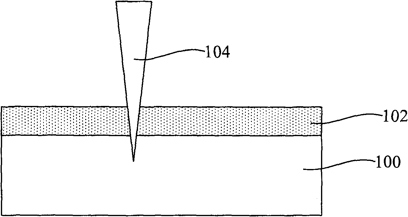
[0007] However, due to the shallow junction depth of the doped layer of the LDD, for example, in the 65nm process, the junction depth of the LDD can reach 30nm or even smaller. When operating with a probe, the probe can easily penetrate the LDD doped layer. like figure 1 As shown, since the probe 104 has been in contact with the semiconductor substrate 100 below the LDD doped layer 102, the measurement result will be inaccurate and the repeatability will be poor.

Method used


Image

  • Method and structure for impriving the measurment accuracy of LDD doping layer square resistance
  • Method and structure for impriving the measurment accuracy of LDD doping layer square resistance
  • Method and structure for impriving the measurment accuracy of LDD doping layer square resistance

Examples


Embodiment 1

[0069] The first doping ion is indium, the second doping ion is boron, and the second doping layer is a PLDD doping layer.

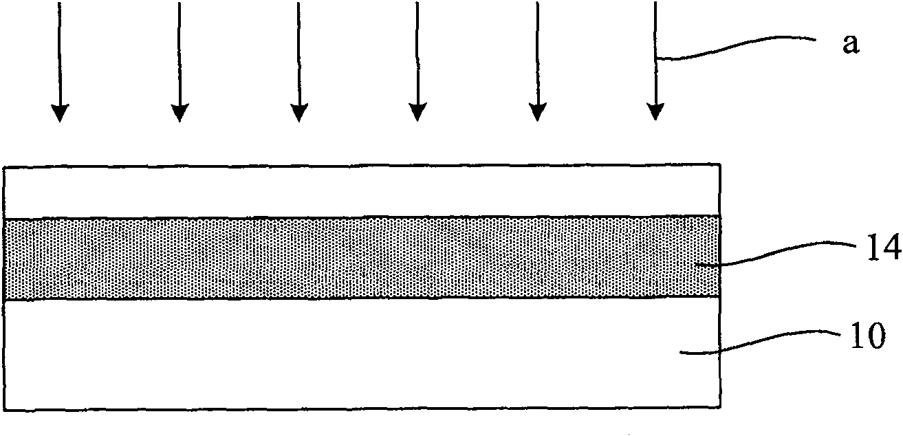
[0070] Such as figure 2 As shown, a semiconductor substrate 10 is provided, which may be monocrystalline silicon or polycrystalline silicon.

[0071] Cleaning the surface of the semiconductor substrate 10 to remove impurity particles, organic or inorganic pollutants, and a natural oxide layer on the surface of the semiconductor substrate 10 .

[0072] Optionally, a thin oxide layer (not shown) can be formed on the surface of the semiconductor substrate 10, which can protect the surface of the semiconductor substrate 10 from contamination and prevent subsequent ion implantation from damaging the semiconductor substrate. The excessive damage of 10 can also be used as an oxidation buffer layer to control the depth of ion implantation.

[0073] Next, a surface pre-amorphous implantation (Pre-Amorphous Implantation, PAI) is performed on the semiconductor s...

Embodiment 2

[0088] The first doping ion is indium, the second doping ion is boron, and the second doping layer is a PLDD doping layer.

[0089] Provide a semiconductor substrate 20, such as Figure 6 As shown in the schematic cross-sectional view, the semiconductor substrate 20 may be single crystal silicon or polycrystalline silicon. Cleaning the surface of the semiconductor substrate 20 to remove impurity particles, organic or inorganic pollutants, and a natural oxide layer on the surface of the semiconductor substrate 20 .

[0090] Perform surface pre-amorphization implantation on the semiconductor substrate 20 to make the surface of the semiconductor substrate 20 in an amorphized state.

[0091] The surface pre-amorphization silicidation implantation generally uses high-mass ions, for example, the impurity implanted in the pre-amorphization implantation can be one of Ge, Si, and Sb.

[0092] By bombarding the surface of the semiconductor substrate 20 with high-mass ions, the surface...

Embodiment 3

[0103] The first doping ion is indium, the second doping ion is boron, and the second doping layer is a PLDD doping layer.

[0104] Provide a semiconductor substrate 30, such as Figure 7 As shown, the semiconductor substrate 30 may be single crystal silicon or polycrystalline silicon. Cleaning the surface of the semiconductor substrate 30 to remove impurity particles, organic or inorganic pollutants, and a natural oxide layer on the surface of the semiconductor substrate 30 .

[0105] A first doping ion implantation is performed on the semiconductor substrate 30 to form a first doping layer 34 in the semiconductor substrate 30 .

[0106] The first dopant ion is indium, the implanted energy may be 30 to 200KeV, and the dose may be 5×10 12 up to 5×10 13 atom / cm 2 , the inclination angle during injection can be 0 degrees.

[0107] The energy of the first dopant ion implantation is relatively high, and the implantation depth is relatively deep, which is greater than the impl...


PUM


Abstract

A method for improving measurement accuracy of the square resistance of a lightly doped drain (LDD) doped layer comprises the following steps: providing a semiconductor substrate; forming a first doped layer with first doping ions and a second doped layer with second doping ions in the semiconductor substrate, wherein the first doped layer is positioned below the second doped layer and contacts with the second doped layer; annealing the semiconductor substrate with the first doped layer and the second doped layer; and measuring the square resistance of the second doped layer. The invention also provides a structure for improving measurement accuracy of the square resistance of the LDD doped layer. The method can reduce the influence of the substrate on measurement results.

Description

technical field [0001] The invention relates to the technical field of semiconductor manufacturing, in particular to a method and structure for improving the measurement accuracy of the sheet resistance (Sheet Resistivity) of a lightly doped drain (Light Doped Drain, LDD) doped layer. Background technique [0002] With the continuous improvement of complementary metal-oxide-semiconductor transistor (CMOS) technology, the integration level is getting higher and higher, the line width of the gate is getting smaller and smaller, and the length of the conductive channel under the gate structure is also continuously decreasing. [0003] In order to suppress the leakage current between the source and the drain due to the reduction of the length of the conductive channel, the LDD implantation process is introduced, that is, before the heavy doping of the source and the drain, ions with a larger molecular weight are first used Perform a shallow junction implant. [0004] In the LDD...

Claims


Application Information

Patent Timeline
Patent Type & Authority Patents(China)
IPC IPC(8): H01L21/66H01L21/265H01L21/336H01L29/02
Inventor 何永根
Owner SEMICON MFG INT (SHANGHAI) CORP
Learn More