Chip packaging method and packaging structure

A chip packaging structure and chip packaging technology, applied in the direction of semiconductor/solid-state device parts, semiconductor devices, electrical components, etc., can solve the problems of increased difficulty of plastic packaging process, thickness limitation of stacked packaging structure, etc., to simplify process complexity, The effect of reducing thickness and simplifying process difficulty

Active Publication Date: 2017-11-24
SILERGY SEMICON TECH (HANGZHOU) CO LTD
View PDF6 Cites 3 Cited by
  • Summary
  • Abstract
  • Description
  • Claims
  • Application Information

AI Technical Summary

Problems solved by technology

However, whether it is a stacked package realized by wire bonding technology or a stacked package realized by flip chip technology, it is necessary to use leads or bumps on the chip to lead out the electrodes of the chip, so that the thickness of the stacked package structure is reduced. small limited by larger
Moreover, in some stacked packages, the difficulty of the plastic packaging process will further increase

Method used


Image

  • Chip packaging method and packaging structure
  • Chip packaging method and packaging structure
  • Chip packaging method and packaging structure

Examples


Embodiment Construction

[0040] Hereinafter, the present invention will be described in more detail with reference to the accompanying drawings. In the various drawings, the same components are denoted by similar reference numerals. For the sake of clarity, various parts in the drawings have not been drawn to scale. Also, some well-known parts may not be shown. For simplicity, the structure obtained after several steps can be described in one figure. In the following, many specific details of the present invention are described, such as the structure, material, size, process and technique of each constituent part, for a clearer understanding of the present invention. However, the invention may be practiced without these specific details, as will be understood by those skilled in the art. In addition, in this application, a chip refers to a semiconductor bare chip.

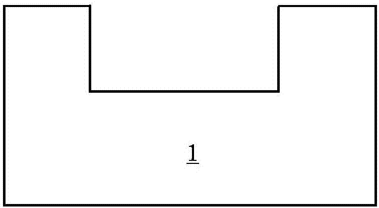
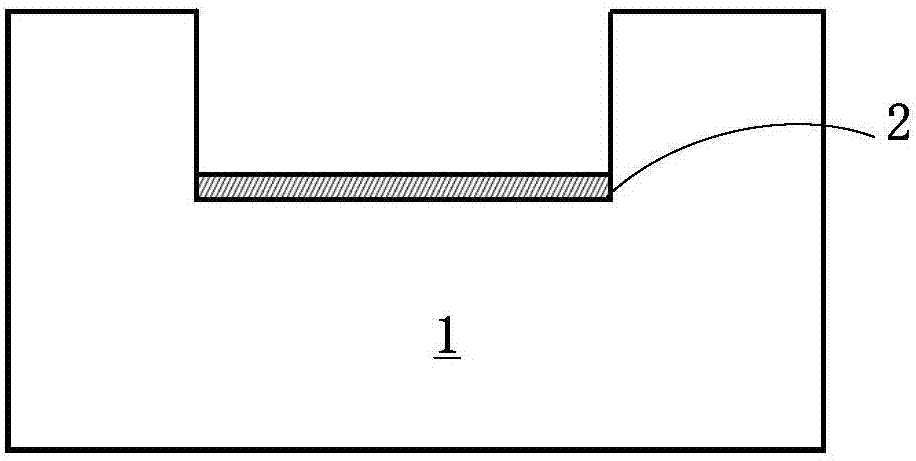
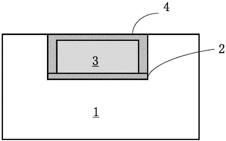
[0041] The present invention provides a chip packaging method, which mainly includes forming a first cavity in a substrate, and insta...


PUM


Abstract

The invention provides a chip packaging method and a packaging structure. The chip packaging method comprises the steps of forming a cavity in a base body; and then installing a chip in the cavity, wherein the base body encapsulates the installed chip to serve as a protective shell of the installed chip. Therefore, a traditional plastic packaging process is not needed to be adopted to form a plastic package body for protecting the chip, and the technical complexity of the chip packaging structure is simplified efficiently. In addition, the base body also serves as a carrier of the installed chip, so that the chip is not needed to be installed at a pre-formed lead frame; and a bonding wire is not required to be adopted and convex points are not needed to be formed on the chip in the process of leading out a chip electrode, so that the technical difficulty is not only further simplified, but also the thickness of the chip packaging structure can be reduced efficiently.

Description

technical field [0001] The invention relates to the technical field of semiconductors, in particular to a chip packaging method and packaging structure. Background technique [0002] With the increasing demand for miniaturization, thinning and high integration of electronic components, there are higher and higher requirements for the packaging area and thickness of semiconductors. [0003] The packaging method that appeared in the early days mainly used wire bonding technology to realize the lead-out of chip electrodes. Although this packaging method is mature and easy to produce, the height of the lead usually needs to be significantly higher than the height of the chip, making the packaging thickness of the chip Larger, and the packaging area is also larger. In order to reduce the thickness and area of ​​chip packaging, flip-chip packaging technology is widely used. However, flip-chip packaging technology needs to make conductive bumps on the chip and metal layers under t...

Claims


Application Information

Patent Timeline
Patent Type & Authority Applications(China)
IPC IPC(8): H01L21/52H01L21/54H01L23/488H01L23/053H01L25/10
CPCH01L21/52H01L21/54H01L23/053H01L24/16H01L25/105H01L2224/02373H01L2224/02381H01L2224/0233H01L2224/0231H01L2224/16057H01L2224/19H01L2224/04105H01L2224/73267H01L2224/92244H01L2924/15153H01L23/13H01L23/5389H01L23/49827H01L23/04H01L23/24H01L25/0657H01L2225/06548H01L2225/06572H01L2225/06527H01L2225/06589H01L2225/06555H01L2225/06558H01L23/4951H01L23/4952H01L23/49513H01L23/3114H01L23/49575
Inventor 陈世杰
Owner SILERGY SEMICON TECH (HANGZHOU) CO LTD
Why Eureka
Try Eureka