Method for manufacturing bonded wafer with ultra-thin single crystal ferroelectric film

a technology of ferroelectric film and bonded wafer, which is applied in the direction of manufacturing tools, polycrystalline material growth, after-treatment details, etc., can solve the problems of clipping and loading, commercialized single crystal ferroelectric wafer with 300 500 um in thickness cannot meet the requirements of advanced communication devices, and manufacture wafers of at least several hundred micrometers in thickness, etc., to achieve the effect of reducing the yield of the process and easy breaking

Inactive Publication Date: 2006-05-04
IND TECH RES INST
View PDF4 Cites 3 Cited by
  • Summary
  • Abstract
  • Description
  • Claims
  • Application Information

AI Technical Summary

Benefits of technology

[0009] 3. The conventional method has no carrier wafer to hold the produced ultra-thin single crystal ferroelectric film such that the single crystal ferroelectric film is easily broken and thus the yield of the process is reduced.

Problems solved by technology

The current commercialized single crystal ferroelectric wafer with about 300˜500 um in thickness can no longer satisfy the requirements of advanced communication devices.
The conventional wafer process can only manufacture wafers of at least several hundred micrometers in thickness, or else the clipping and loading issues have to be overcome while manufacturing ultra-thin wafers.
Moreover, the thin wafers are easily broken during the posterior processes.
The conventional method adopts the process of single crystal ion cutting such that the cost of equipments required in the process is increased and thus the competitiveness is decreased.
The control conditions of the conventional method are much stricter, that cause the process to be much complicated and has affect on the capability of mass production.
The conventional method has no carrier wafer to hold the produced ultra-thin single crystal ferroelectric film such that the single crystal ferroelectric film is easily broken and thus the yield of the process is reduced.

Method used


Image

  • Method for manufacturing bonded wafer with ultra-thin single crystal ferroelectric film
  • Method for manufacturing bonded wafer with ultra-thin single crystal ferroelectric film
  • Method for manufacturing bonded wafer with ultra-thin single crystal ferroelectric film

Examples


Embodiment Construction

[0034] Matched with corresponding drawings, the preferable embodiments of the invention are presented as following and hope they will benefit your esteemed reviewing committee members in reviewing this patent application favorably.

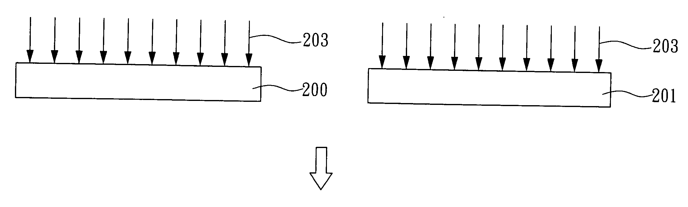
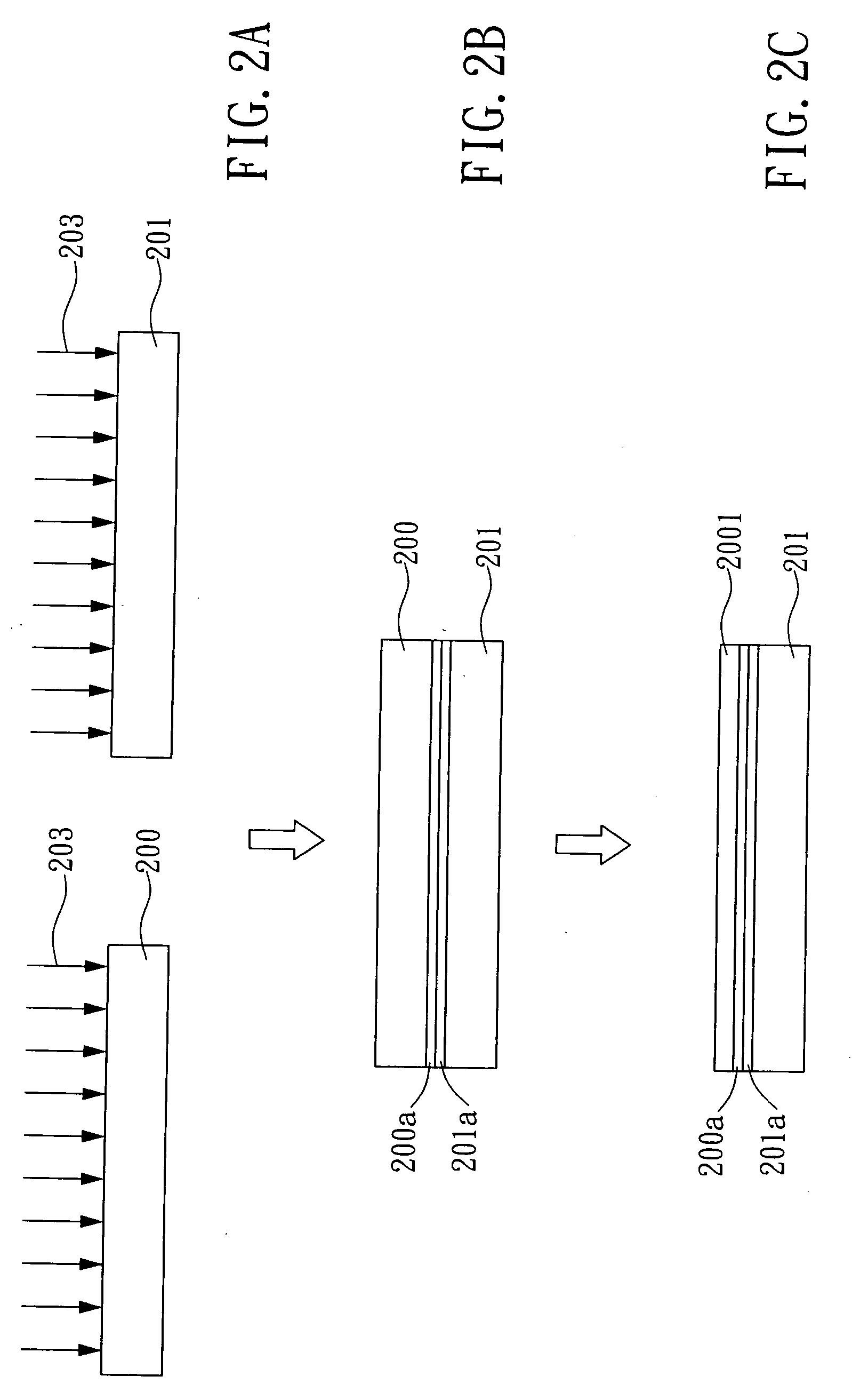
[0035] Please refer to FIG. 2A to FIG. 2C, which shows the first preferred embodiment of the method for manufacturing a bonded wafer with ultra-thin single crystal ferroelectric film according to the present invention.

[0036] As shown in the FIG. 2A, a single crystal ferroelectric wafer 200 and a carrier wafer 201 are provided. Wherein the material of the single crystal ferroelectric wafer 200 can be Lithium Niobate, Lithium Tantalate, or Barium Titanate and so on, and the material of the carrier wafer 201 can be the same as or different to that of the single crystal ferroelectric wafer 200. Then plasma 203 is used to activate the surfaces of the single crystal ferroelectric wafer 200 as well as the carrier wafer 201. It is obviously that the plasma 203 c...


PUM

PropertyMeasurementUnit
thicknessaaaaaaaaaa
thicknessaaaaaaaaaa
ferroelectricaaaaaaaaaa

Abstract

A method for manufacturing a bonded wafer with ultra-thin single crystal ferroelectric film is provided, comprising the following steps: providing a single crystal ferroelectric wafer and a carrier wafer while activating the surfaces of the single crystal ferroelectric wafer and the carrier wafer; bonding the activated surface of the single crystal ferroelectric wafer to the activated surface of the carrier wafer; and thinning the single crystal ferroelectric wafer for forming an ultra-thin single crystal ferroelectric film. Wherein, the thinning process in the aforesaid preferred embodiment is the method of polishing, grinding, chemical mechanical polishing, or etching. And the bonding force generated in the bonding process is strong enough to resist the shearing force.

Description

FIELD OF THE INVENTION [0001] The present invention relates to a method for manufacturing bonded wafer with ultra-thin single crystal ferroelectric film, and more particularly, to a method combined with wafer bonding and wafer thinning for manufacturing a bonded wafer with ultra-thin single crystal ferroelectric film. BACKGROUND OF THE INVENTION [0002] Accompanied with the trend of communication using broader band and higher frequency, the performance of related audio and optical communication devices have to be largely improved. Since the single crystal ferroelectric materials have excellence photoelectric characteristics, they are widely used in the audio and optical communication devices. [0003] The current commercialized single crystal ferroelectric wafer with about 300˜500 um in thickness can no longer satisfy the requirements of advanced communication devices. In the recent research reports, a high performance device of which the frequency is 3˜4 times faster than that of the ...

Claims


Application Information

Patent Timeline
Patent Type & Authority Applications(United States)
IPC IPC(8): C30B23/00C30B25/00C30B28/12C30B28/14C30B29/30C30B29/32C30B33/06H01L21/02
CPCC30B29/30C30B29/32C30B33/06
Inventor HO, SHIH-SHIANTSAI, HUNG-YINTING, CHIA-JENLAN, CHUN-FACHEN, CHIJ-CHANG
Owner IND TECH RES INST
Why Eureka
Try Eureka