
Optical filter and device using optical filter

An optical filter and wavelength technology, used in optics, optical components, optical components, etc., can solve the problem of inability to obtain a wide viewing angle value, etc., achieves excellent reduction effect of multiple reflected light, small incident angle dependence, and excellent cut-off characteristics. Effect

Active Publication Date: 2020-02-07
JSR CORPORATIOON
View PDF31 Cites 0 Cited by
  • Summary
  • Abstract
  • Description
  • Claims
  • Application Information

AI Technical Summary

Problems solved by technology

The near-infrared cut filter described in Patent Document 2 is excellent in near-infrared cut characteristics, moisture absorption resistance, and impact resistance, but cannot achieve a wide viewing angle value.

Method used


Image

  • Optical filter and device using optical filter
  • Optical filter and device using optical filter
  • Optical filter and device using optical filter

Examples


Embodiment

[0255] Hereinafter, the present invention will be more specifically described based on examples, but the present invention is not limited by these examples. In addition, "part" means a "weight part" unless otherwise specified. In addition, the measurement method of each physical property value and the evaluation method of a physical property are as follows.

[0256]

[0257] The molecular weight of the resin is measured by the method of the following (a) or the following (b) considering the solubility of each resin with respect to a solvent, etc.

[0258] (a) Gel Permeation Chromatography (GPC) device (150C type, column: H type column produced by Tosoh (Tosoh) Company, developing solvent: o-dichlorobenzene) manufactured by Waters (WATERS) Company, The weight average molecular weight (Mw) and the number average molecular weight (Mn) of standard polystyrene conversion were measured.

[0259] (b) Using a GPC device manufactured by Tosoh Corporation (HLC-8220 type, column: TSK...

Synthetic example

[0273] Compound (A) and compound (S) used in the following examples were synthesized by generally known methods. As a common synthesis method, for example, Japanese Patent No. 3366697, Japanese Patent No. 2846091, Japanese Patent No. 2864475, Japanese Patent No. 3703869, Japanese Patent Laid-Open No. 60-228448, Japanese Japanese Patent Laid-Open No. 1-146846, Japanese Patent Laid-Open No. 1-228960, Japanese Patent No. 4081149, Japanese Patent Laid-Open No. 63-124054, "Phthalocyanine-Chemistry and Function-" (IPC, 1997 2007-169315), Japanese Patent Laid-Open No. 2009-108267, Japanese Patent Laid-Open No. 2010-241873, Japanese Patent No. 3699464, Japanese Patent No. 4740631, etc. Methods.

Synthetic example 1

[0275] The 8-methyl-8-methoxycarbonyltetracyclo[4.4.0.1 represented by the following formula (a) 2,5 .1 7,10 ] 100 parts of dodec-3-ene (hereinafter also referred to as "DNM"), 18 parts of 1-hexene (molecular weight modifier) ​​and 300 parts of toluene (solvent for ring-opening polymerization reaction) were added to the reaction vessel replaced by nitrogen , and the solution was heated to 80°C. Then, 0.2 parts of a toluene solution (0.6 mol / L) of triethylaluminum as a polymerization catalyst and a toluene solution (0.025 mol / L) of methanol-modified tungsten hexachloride were added to the solution in the reaction vessel 0.9 parts, and the solution was heated and stirred at 80° C. for 3 hours, thereby performing a ring-opening polymerization reaction to obtain a ring-opening polymer solution. The polymerization conversion rate in the polymerization reaction was 97%.

[0276] [chemical 20]

[0277]

[0278] 1,000 parts of the ring-opening polymer solution obtained in the m...


PUM

PropertyMeasurementUnit
absorption wavelengthaaaaaaaaaa
thicknessaaaaaaaaaa
glass transition temperatureaaaaaaaaaa

Abstract

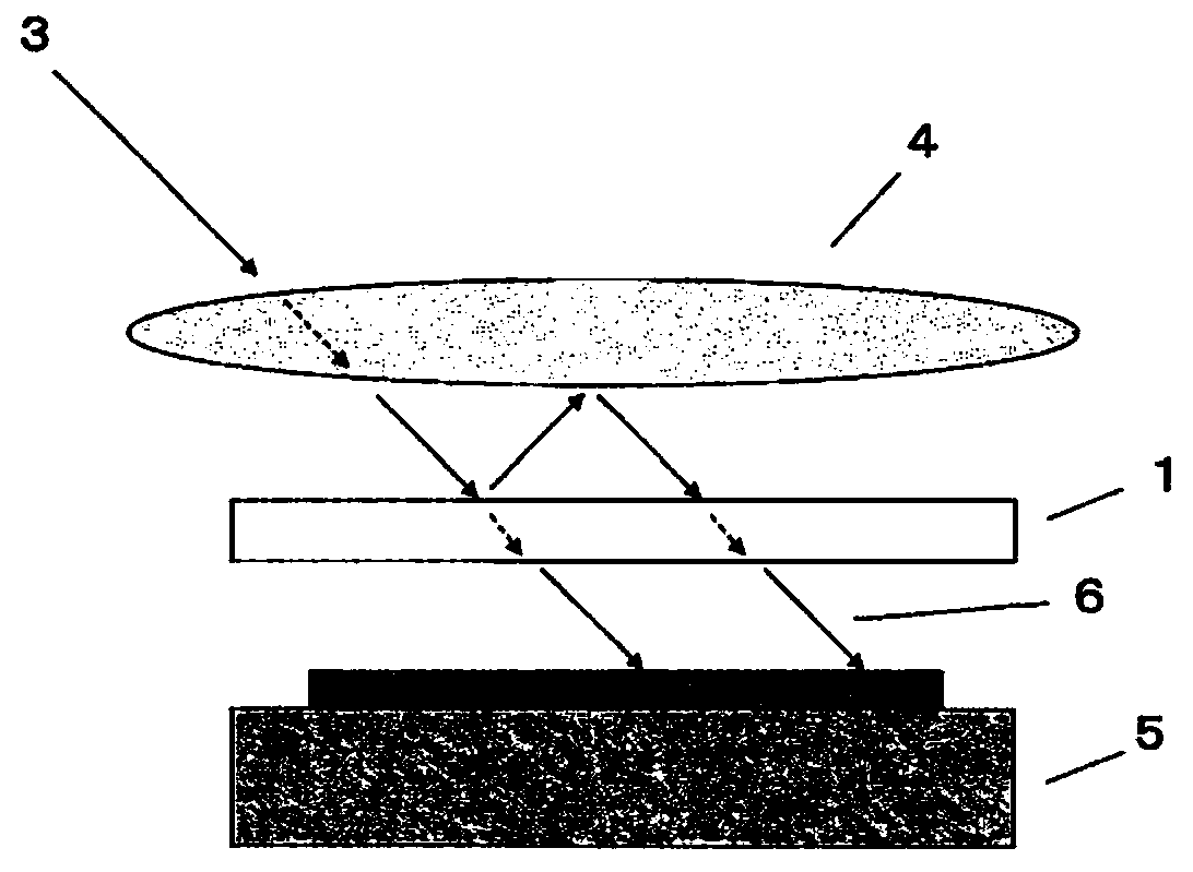
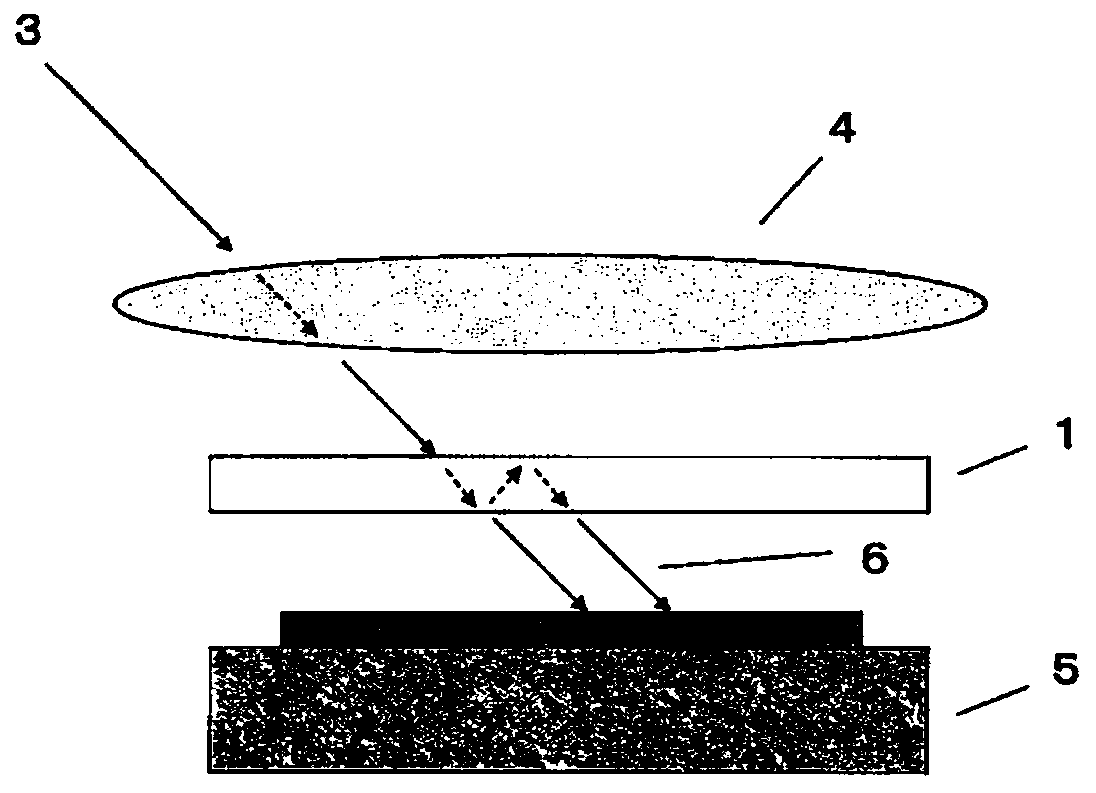
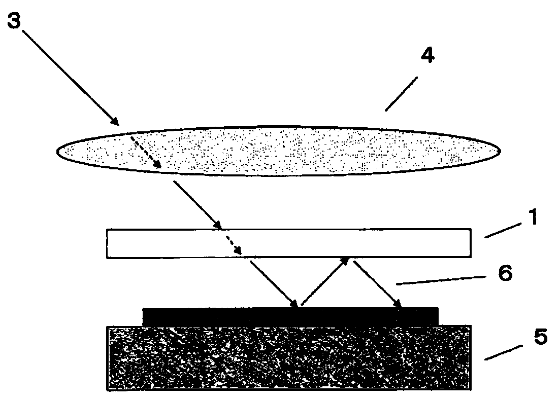
The subject of the present invention is to provide an optical filter and a device using the optical filter which have little dependence on the incident angle and can reduce multiple reflections when near-infrared light is incident from an oblique direction. The optical filter of the present invention is characterized in that it includes a substrate and a dielectric multilayer film formed on at least one surface of the substrate, and the substrate contains a compound (A ), and a transparent resin layer having a compound (S) having a maximum absorption in a wavelength of 750 nm or more and 1050 nm or less, or having a transparent resin layer containing the compound (A) and a transparent resin layer containing the compound (S) , to satisfy the following requirement (a): (a) in the region of wavelength 800nm~1000nm, the average value of the transmittance when measured from the vertical direction of the optical filter is 5% or less.

Description

technical field [0001] The invention relates to an optical filter and a device using the optical filter. Specifically, the present invention relates to an optical filter containing a compound that absorbs in a specific wavelength range, and a solid-state imaging device and camera module using the optical filter. Background technique [0002] In solid-state imaging devices such as video cameras, digital still cameras, and mobile phones with camera functions, charge-coupled device (CCD) image sensors or complementary metal-oxide-semiconductor (Complementary Metal Oxide Semiconductor (CMOS) image sensors, these solid-state imaging elements use silicon photodiodes (silicon photodiodes) sensitive to near-infrared rays that cannot be detected by human eyes in their light-receiving parts. In these solid-state imaging devices, it is necessary to perform visibility correction to present a natural color to the human eye, and an optical filter (such as a near-infrared cut filter) that...

Claims


Application Information

Patent Timeline
Patent Type & Authority Patents(China)
IPC IPC(8): G02B5/22G02B5/28
CPCG02B5/22G02B5/28B32B7/023B32B27/08B32B27/28B32B2307/412B32B2551/00
Inventor 长屋胜也重冈大介堀内正子葛西达也
Owner JSR CORPORATIOON
Learn More