Organic light-emitting display panel and manufacturing method thereof, and electronic equipment

A light-emitting display and organic technology, applied in semiconductor/solid-state device manufacturing, circuits, electrical components, etc., can solve the problems of occupying display area, affecting manufacturing cost and device reliability, and deteriorating user experience, so as to improve fingerprint recognition Accuracy, reduced manufacturing process, and increased area

Active Publication Date: 2017-12-01
WUHAN TIANMA MICRO ELECTRONICS CO LTD
View PDF3 Cites 48 Cited by
  • Summary
  • Abstract
  • Description
  • Claims
  • Application Information

AI Technical Summary

Problems solved by technology

[0003] In the existing display device with fingerprint recognition function, the fingerprint recognition sensor is a separate component, or it is placed on the front of the display device to occupy the area of ​​the display screen, or it is placed on the back of the dis

Method used


Image

  • Organic light-emitting display panel and manufacturing method thereof, and electronic equipment
  • Organic light-emitting display panel and manufacturing method thereof, and electronic equipment
  • Organic light-emitting display panel and manufacturing method thereof, and electronic equipment

Examples


Example Embodiment

[0026] In order to make the objectives, technical solutions and advantages of the present invention clearer, the following will refer to the accompanying drawings in the embodiments of the present invention, and describe the technical solutions of the present invention clearly and completely through the implementation manner. Obviously, the described embodiments are the present invention. Some examples, but not all examples. Based on the embodiments of the present invention, all other embodiments obtained by those of ordinary skill in the art without creative efforts shall fall within the protection scope of the present invention.
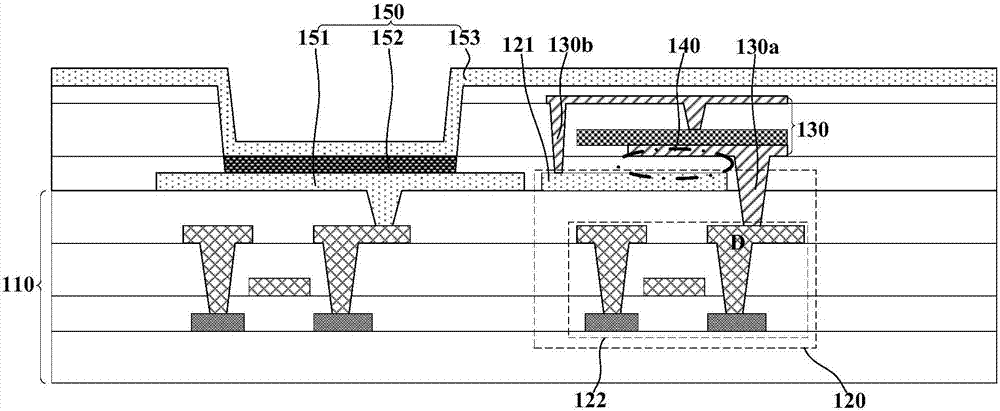
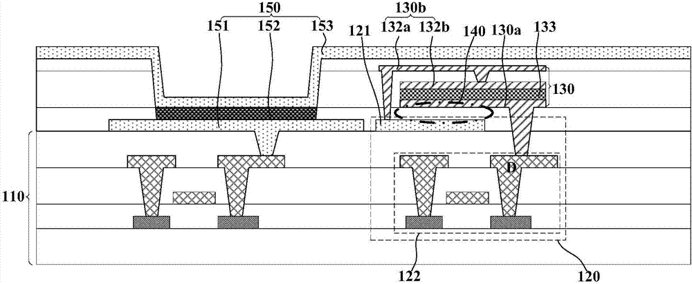
[0027] refer to Figure 1A As shown, it is a schematic diagram of an organic light-emitting display panel provided by an embodiment of the present invention. The organic light emitting display panel according to the embodiment of the present invention includes: an array substrate 110, and a light-sensing recognition array located on the array subs...


PUM


Abstract

Embodiments of the invention disclose an organic light-emitting display panel and a manufacturing method thereof, and electronic equipment. The organic light-emitting display panel comprises an array substrate, a photosensitive recognition array, and photosensitive detection circuits, the photosensitive recognition array comprises a plurality of photosensitive recognition devices, each photosensitive detection circuit comprises a common voltage input layer and a photosensitive detection switch, the photosensitive detection switch comprises a drain electrode metal layer, a first electrode of the photosensitive recognition device is electrically connected with the drain electrode metal layer of the corresponding photosensitive detection circuit, a second electrode of the photosensitive recognition device is electrically connected with the common voltage input layer of the corresponding photosensitive detection circuit, the common voltage input layer and the first electrode of the corresponding photosensitive recognition device are overlapped in a direction vertical to the array substrate, or the common voltage input layer and the drain electrode metal layer of the photosensitive detection circuit are overlapped in the direction vertical to the array substrate to form a photosensitive storage capacitor. According to the organic light-emitting display panel and the manufacturing method thereof, and the electronic equipment, the function of embedded fingerprint recognition is realized by the organic light-emitting display panel, and the effect of fingerprint touch control is realized.

Description

technical field [0001] Embodiments of the present invention relate to display technologies, and in particular to an organic light emitting display panel, a manufacturing method thereof, and electronic equipment. Background technique [0002] Fingerprints are inherent to each person and are unique. With the development of technology, a variety of display devices with fingerprint recognition functions appear on the market, such as mobile phones, tablet computers, and smart wearable devices. In this way, when a user operates a display device with a fingerprint recognition function, he only needs to touch the fingerprint recognition sensor of the display device with his finger to perform fingerprint recognition. [0003] In the existing display device with fingerprint recognition function, the fingerprint recognition sensor is a separate component, or it is placed on the front of the display device to occupy the area of ​​the display screen, or it is placed on the back of the d...

Claims


Application Information

Patent Timeline
IPC IPC(8): H01L27/32H01L51/52H01L51/56
CPCH10K59/60H10K59/40H10K50/80H10K71/00H01L27/14678G06V40/1318G06V40/12H10K59/65
Inventor 丁洪杨康杜凌霄曾洋王丽花姚绮君
Owner WUHAN TIANMA MICRO ELECTRONICS CO LTD
Why Eureka
Try Eureka