

Printed circuit board
A printed circuit board and circuit technology, applied in the field of multi-layer printed circuit board strain testing of printed circuit board components, can solve the problems of easy disconnection of connecting lines, reduced effectiveness of stress testing, and reduced accuracy of test results, etc. The effect of high coverage, improved effectiveness and accuracy
- Summary
- Abstract
- Description
- Claims
- Application Information
AI Technical Summary
Problems solved by technology
Method used
Image

Examples
Embodiment Construction
[0019] The technical solutions in the embodiments of the present invention will be clearly and completely described below in conjunction with the accompanying drawings. Apparently, the described embodiments are only some of the embodiments of the present invention, but not all of them. Based on the embodiments of the present invention, all other embodiments obtained by persons of ordinary skill in the art without making creative efforts belong to the protection scope of the present invention.
[0020] The structure of the PCB board described in the embodiment of the present invention is to illustrate the technical solution of the embodiment of the present invention more clearly, and does not constitute a limitation to the technical solution provided by the embodiment of the present invention. The technical solutions provided by the embodiments of the present invention are also applicable to similar technical problems when the scene arises.
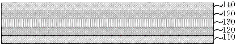
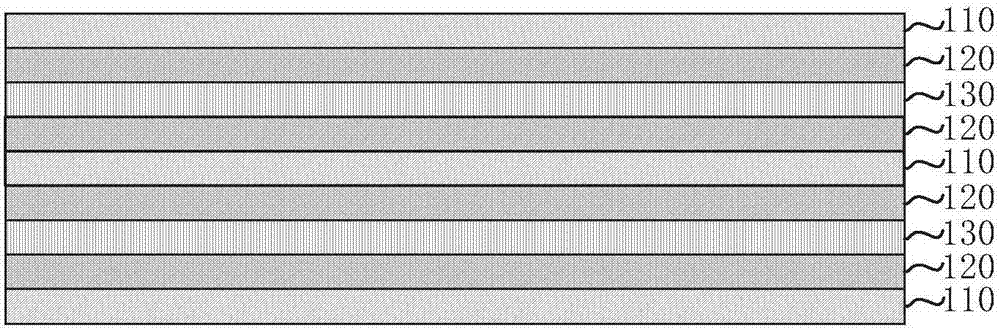
[0021] Such as figure 1 as shown,...
PUM
 Abstract
Description
Claims
Application Information