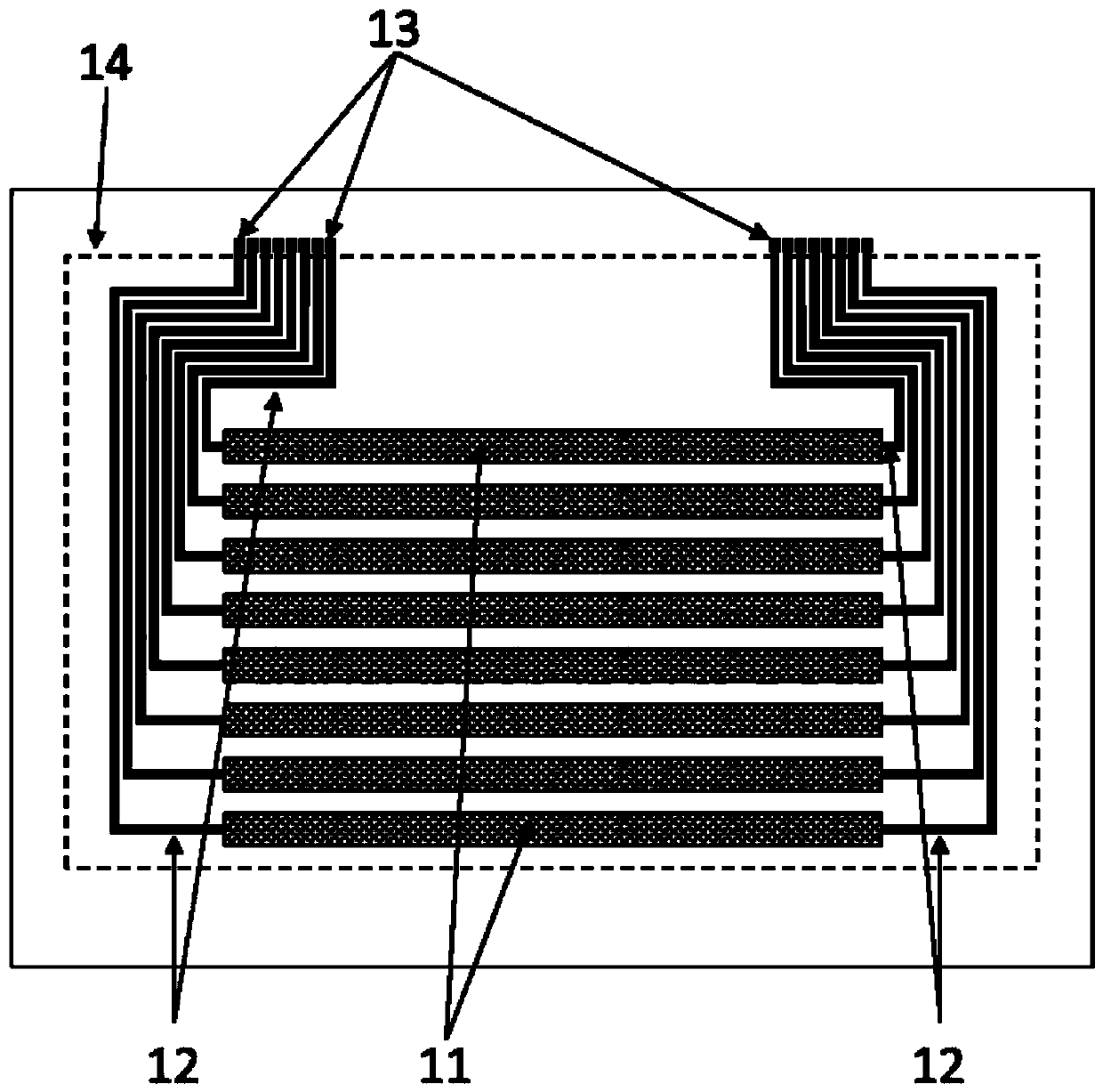
Light-transmitting electrode laminate
An electrode layer and light-transmitting technology, applied to the conductive layer on the insulating carrier, layered products, metal layered products, etc., can solve problems such as insufficient methods, achieve excellent reliability, and suppress changes in resistance value
- Summary
- Abstract
- Description
- Claims
- Application Information
AI Technical Summary
Problems solved by technology
Method used
Image
Examples
Embodiment
[0149] Hereinafter, the present invention will be described in detail using examples. However, the present invention is not limited to the following examples, and various modifications and changes are possible unless the gist of the present invention is exceeded.
[0150] Fabrication of light-transmitting electrode 1
[0151] As the support, a polyethylene terephthalate film with a thickness of 100 μm was used. In addition, the total light transmittance of this support was 91.5%.
[0152] Next, a base layer of the composition described below was coated on the support, dried, and a physical development core layer was provided.
[0153] Preparation of palladium sulfide sol
[0154]
[0155] Liquid A and liquid B were mixed while stirring, and passed through a column filled with an ion exchange resin after 30 minutes to obtain a palladium sulfide sol.
[0156] Substrate composition / square meter
[0157]
[0158]
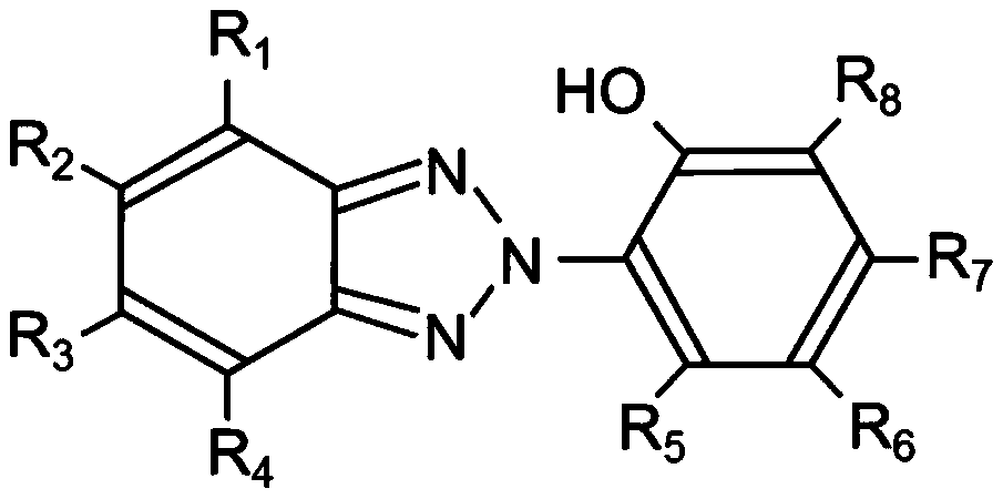
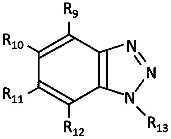
[0159] [chem 29]
[0160]
[0161] On the base la...
PUM
| Property | Measurement | Unit |
|---|---|---|
| width | aaaaa | aaaaa |
| thickness | aaaaa | aaaaa |
| thickness | aaaaa | aaaaa |
Abstract
Description
Claims
Application Information
 - R&D
- Intellectual Property
- Life Sciences
- Materials
- Tech Scout
- Unparalleled Data Quality
- Higher Quality Content
- 60% Fewer Hallucinations
Browse by: Latest US Patents, China's latest patents, Technical Efficacy Thesaurus, Application Domain, Technology Topic, Popular Technical Reports.
© 2025 PatSnap. All rights reserved.Legal|Privacy policy|Modern Slavery Act Transparency Statement|Sitemap|About US| Contact US: help@patsnap.com


