Method for screening out abnormal crystal grains

A grain and abnormal technology, applied in semiconductor/solid state device testing/measurement, electrical components, circuits, etc. The effect of missing detection, reducing customer complaint rate and improving work efficiency

Active Publication Date: 2017-12-15
ANHUI SANAN OPTOELECTRONICS CO LTD
View PDF5 Cites 4 Cited by
  • Summary
  • Abstract
  • Description
  • Claims
  • Application Information

AI Technical Summary

Problems solved by technology

For example, if the grains that are electrostatically broken down after the ESD test are sampled, they need to be picked out through the appearance microscope because they will not pass the electrical screening of the whole test. However, when the appearance of the grains is damaged or not depends entirely on manual judgment, the grain It is difficult to have a unified standard for the appearance loss of grains. Manual microscope inspection often fails to detect, especially the grains with burst points, which is the main reason for customer complaints.
[0003] Therefore, a new screening method has been found, which can effectively screen out the grains of electrostatic breakdown, reduce the low detection rate of sporadic appearance problems caused by electrical abnormalities, and affect product quality.

Method used


Image

  • Method for screening out abnormal crystal grains
  • Method for screening out abnormal crystal grains
  • Method for screening out abnormal crystal grains

Examples


Embodiment Construction

[0027] In the following paragraphs the invention is described more specifically by way of example with reference to the accompanying drawings. Advantages and features of the present invention will be apparent from the following description and claims. It should be noted that all the drawings are in a very simplified form and use imprecise scales, and are only used to facilitate and clearly assist the purpose of illustrating the embodiments of the present invention.

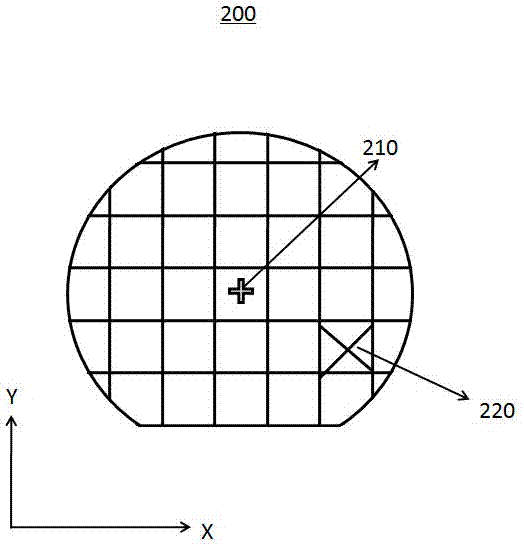
[0028] Sampling in the present invention refers to testing part of the crystal grains in the whole wafer, and the sampling map is formed according to the positions of the sampling grains. The full test refers to testing all the dies on the wafer, and the full test map is formed according to the positions of the full test dies.

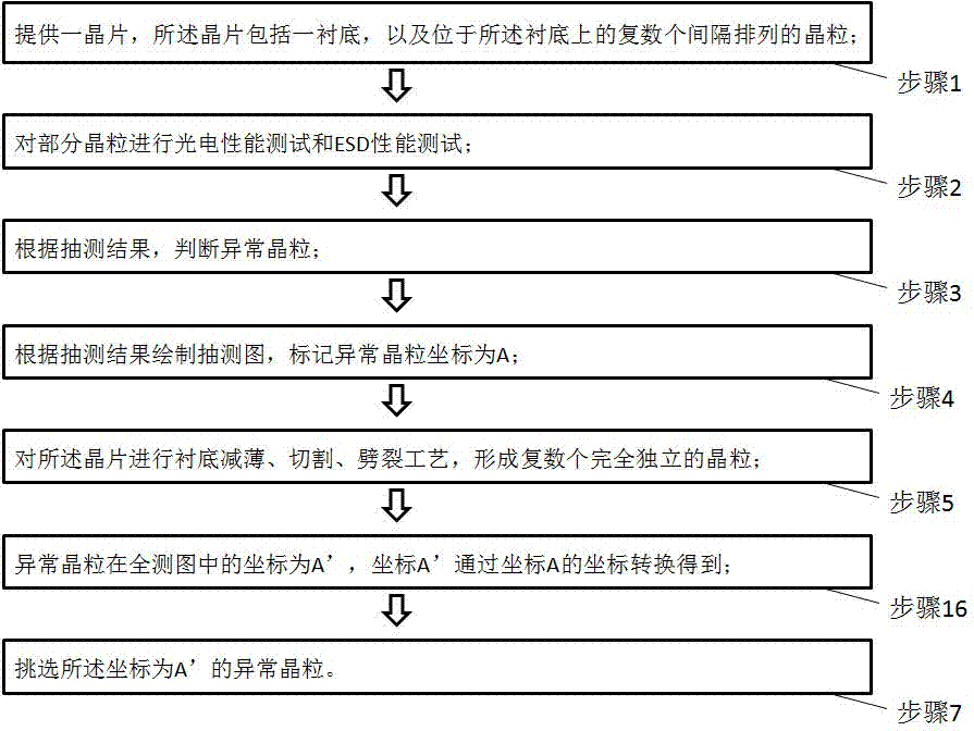
[0029] See attached figure 1 , a method for screening abnormal crystal grains provided by the present invention, at least includes the following steps:

[0030] Step 1, providing a wafe...


PUM


Abstract

The invention belongs to the field of semiconductors, and especially relates to a method for screening out the abnormal crystal grains through the photoelectric property parameters of the crystal grains. The method achieves the screening of the abnormal crystal grains through the testing of the photoelectric properties of the crystal grains and a method of coordinate conversion of crystal grains, improves the work efficiency of a crystal grain mirror, reduces the detection leakage, reduces the complaint rate of customers, and improves the work efficiency.

Description

technical field [0001] The invention belongs to the field of semiconductor luminescence, and in particular relates to a method for screening abnormal grains. Background technique [0002] GaN-based materials are ideal materials for short-wavelength light-emitting devices, and their applications cover white lighting, backlighting, and display screens. With the improvement of epitaxial technology capabilities, the concentration of grain output has been greatly improved. The grain incomplete measurement and non-sorting process has a significant cost-effectiveness for grain production and packaging manufacturers, but there are some difficulties in the implementation of this process. For example, if the grains that are electrostatically broken down after the ESD test are sampled, they need to be picked out through the appearance microscope because they will not pass the electrical screening of the whole test. However, when the appearance of the grains is damaged or not depends en...

Claims


Application Information

Patent Timeline
IPC IPC(8): H01L21/66H01L21/67
Inventor 范慧丽黄瀚毅孙旭张家宏
Owner ANHUI SANAN OPTOELECTRONICS CO LTD
Why Eureka
Try Eureka