Display panel and display device
A technology for display panels and array substrates, applied in identification devices, static indicators, instruments, etc., can solve the problems of small design space of two-dimensional codes and excessive wiring of ESD circuit signals
- Summary
- Abstract
- Description
- Claims
- Application Information
AI Technical Summary
Problems solved by technology
Method used
Image
Examples
Embodiment Construction
[0028] Aiming at the problems existing in the prior art that the ESD circuit and some signal traces exceed the cutting line due to the compression of the lower frame size, and the design space of the two-dimensional code is small, the embodiment of the present invention provides a display panel and a display device .
[0029] The specific implementation manners of the display panel and the display device provided by the embodiments of the present invention will be described in detail below with reference to the accompanying drawings. The size and shape of each structure in the drawings do not reflect the real scale, but are only intended to schematically illustrate the content of the present invention.
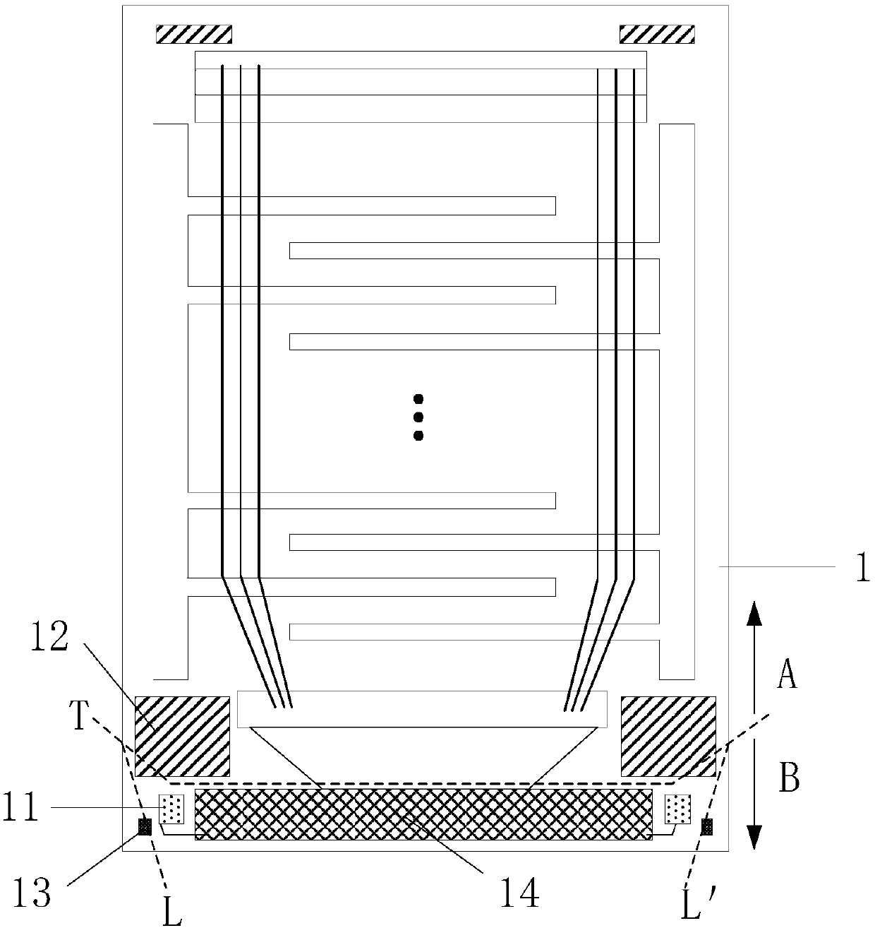
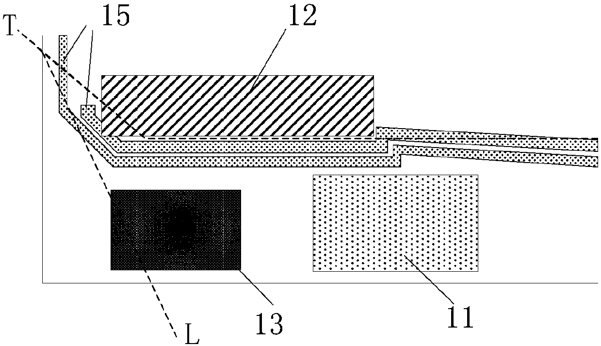
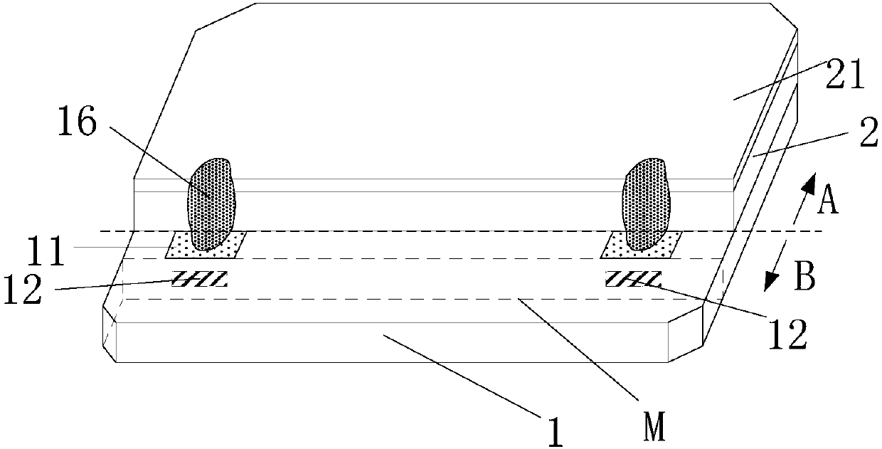
[0030] An embodiment of the present invention provides a display panel, such as Figure 2a As shown, it includes: an array substrate 1, and an opposite substrate 2 arranged opposite to the array substrate 1; wherein,
[0031] The array substrate 1 includes: a facing area tha...
PUM
 Abstract
Description
Claims
Application Information


