Area array routing masks for improved escape of devices on PCB

A technology of area and array, applied in the field of area array wiring mask

Inactive Publication Date: 2007-04-04
ALCATEL LUCENT SAS
View PDF0 Cites 7 Cited by
  • Summary
  • Abstract
  • Description
  • Claims
  • Application Information

AI Technical Summary

Problems solved by technology

However, where there are multiple pinout options that are equivalent under these standards, there is an opportunity to consider PCB routing issues and possibly reduce PCB layer count, provided some guidance is provided for this purpose

Method used


Image

  • Area array routing masks for improved escape of devices on PCB
  • Area array routing masks for improved escape of devices on PCB
  • Area array routing masks for improved escape of devices on PCB

Examples


Embodiment Construction

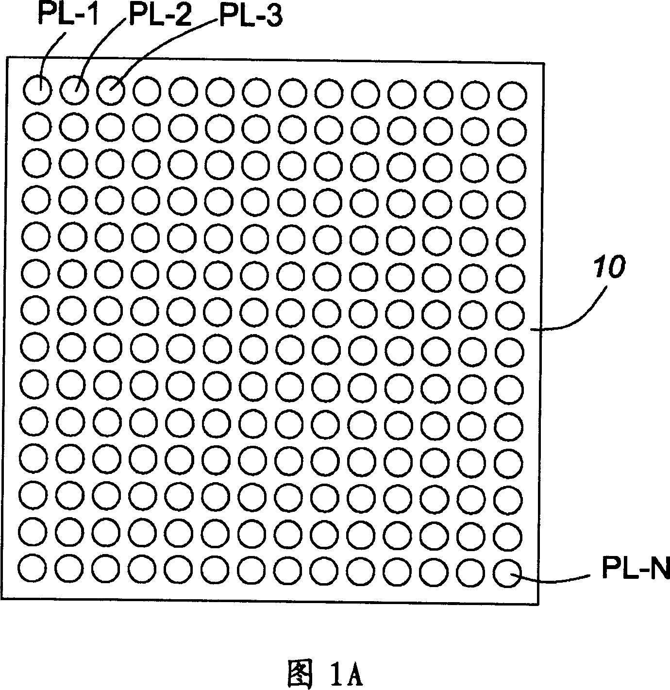
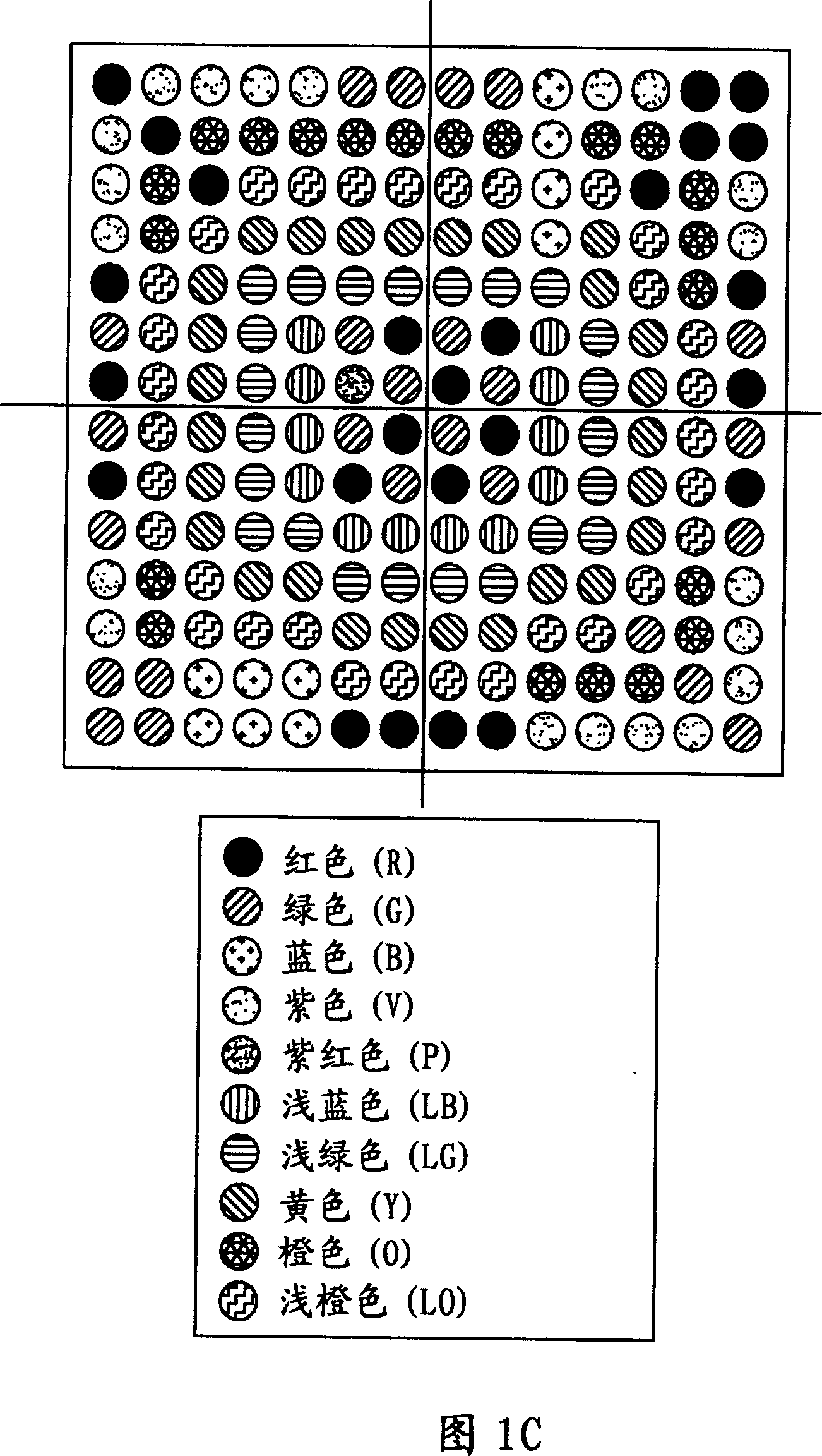
[0035] The invention provides a distribution map package of pins and a determination method thereof. Each map shows areas of the same routing that are easy for a particular package type. For manual pin determination, the same regions are coded with the same color, although they will have the same numerical priority for the automated program. When determining pinouts for a device, the easiest routable area is used first, and then successively fewer routable areas as required, until all pinouts have been assigned. Predetermine locations such as power and ground pins, as well as high-speed buses, clocks, etc. The easiest routable area is usually at the periphery of the package and unless there are any obstacles such as the aforementioned predetermined location, the ease of routable decreases towards the inward layers. Maps can also be provided for no connect (NC) pins to create paths for routing signal traces.

[0036] As an example, a typical PCB is studied. In the worst cas...


PUM


Abstract

A method for optimizing area array device pin utilization and reducing the number of layers on a multilayered PCB comprising: preparing a package of BGA pin-out maps which anticipate the effect of existing fixed pins and derives the resulting optimum pin location assignment. Each pin-out map includes an indication of the best routing for circuits from a given component to be mounted to a PCB. Applying the package of pin-out maps during an area array pin assignment phase, thereby making an area array package capable of supporting the optimum routing configuration proposed by the pin-out maps. Applying the package of pin-out maps during a PCB design phase so that the optimum circuit routing to each pin is achieved, thereby completing the strategy layed out by the proposed pin-out maps, resulting in a lower number of PCB layers.

Description

[0001] References to related patent applications [0002] This application is related to the following U.S. patent applications assigned to the present assignee: [0003] No. 10 / 911,360, filed November 19, 2004, inventor Paul Brown, entitled OFF-WIDTH PITCH FOR IMPROVED CIRCUIT CARD ROUTING; [0004] No.11 / 041,727, filed January 25, 2005, inventor Alex Chan, entitled OFF-GRID DECOUPLING OF BALL GRID ARRAY (BGA) DEVICES; [0005] No. 11 / 200,041, filed August 10, 2005, inventor Paul Brown, entitled USING ROWS / COLUMNS OF MICRO-VIAS TO CREATE PCBROUTING CHANNELS IN BGA INTERCONNECT GRID (Micro-ViaChannels); and [0006] No.11 / 200,044, filed on August 10, 2005, inventor Paul Brown, entitled ALTERNATING MICRO-VIAS AND THROUGHBOARD VIAS TOCREATE PCB ROUTING CHANNELS IN BGA INTERCONNECTGRID. technical field [0007] The present invention relates to PCB technology, and in particular to an area array routing mask for improved escape of devices on a PCB. Background technique [0008...

Claims


Application Information

Patent Timeline
Patent Type & Authority Applications(China)
IPC IPC(8): G06F17/50
CPCH05K3/0005H01L2924/0002H05K1/112H01L23/49838H01L23/49822G06F17/5068H05K2201/10734H05K2201/09227G06F30/39H01L2924/00
Inventor P·J·布朗
Owner ALCATEL LUCENT SAS
Why Eureka
Try Eureka