Unlock instant, AI-driven research and patent intelligence for your innovation.

Method for preparing color-resist layer of array substrate, array substrate and display panel

A technology for array substrates and color-resist layers, applied in microlithography exposure equipment, photolithography exposure devices, instruments, etc., can solve problems such as weak exposure, unstable chemical properties, and affecting the quality of array substrates, and achieve The effect of improving quality and improving stability

Active Publication Date: 2020-07-03
TCL CHINA STAR OPTOELECTRONICS TECH CO LTD
View PDF7 Cites 0 Cited by
  • Summary
  • Abstract
  • Description
  • Claims
  • Application Information

AI Technical Summary

Problems solved by technology

[0003] The inventors of the present invention have found in the long-term research and development that in the current prior art, in order to realize the integration of color filters on the array substrate, the color resistance layer is generally fabricated on the thin film transistor layer, and the color resistance layer is located on the Between the insulating layers, but when the color resist layer is exposed and developed to form the via hole, the exposure to the side wall of the via hole is weak, the color resist crosslinking at this position is insufficient, and the chemical properties are unstable, which seriously affects the array substrate. The follow-up process and the quality of the array substrate

Method used


Image

  • Method for preparing color-resist layer of array substrate, array substrate and display panel
  • Method for preparing color-resist layer of array substrate, array substrate and display panel
  • Method for preparing color-resist layer of array substrate, array substrate and display panel

Examples


Embodiment Construction

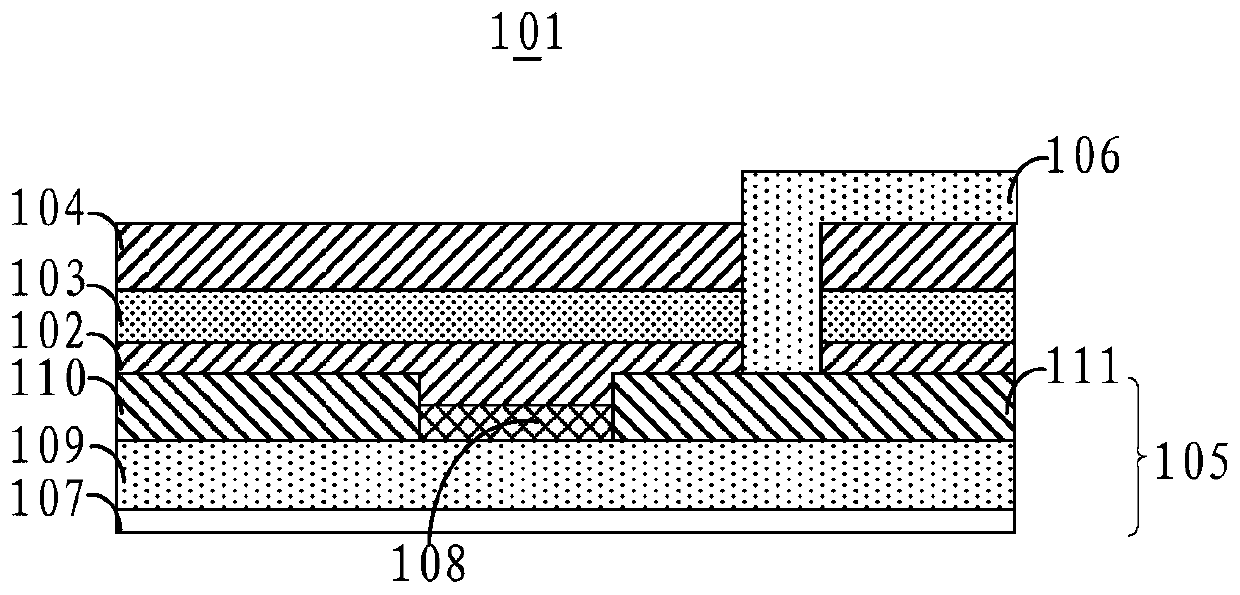
[0019] In the traditional manufacturing process of the display panel, the array substrate and the color filter are arranged separately, and the array substrate and the color filter are bonded through the box-to-box process, but the box-to-box process is prone to light leakage. By disposing the color resist layer on the array substrate, the above light leakage problem can be improved.

[0020] see figure 1 , figure 1 It is a schematic structural diagram of an embodiment of the array substrate of the present invention. The array substrate 101 of this embodiment includes a first passivation layer 102, a color resist layer 103 and a second passivation layer 104 arranged in sequence, wherein the first passivation layer 102, A first through hole (not shown), a second through hole (not shown) and a third through hole (not shown) are respectively formed on the color resist layer 103 and the second passivation layer 104 . Certainly, the array substrate 101 of this embodiment further ...


PUM

PropertyMeasurementUnit
wavelengthaaaaaaaaaa

Abstract

The invention discloses a preparing method of an array substrate color resistance layer, an array substrate and a display panel. The array substrate comprises a first passivation layer, a color resistance layer and a second passivation layer in sequence, and a second through hole is formed in the color resistance layer. The preparing method comprises the steps that the first passivation layer is coated with a color resistance material; the color resistance material is solidified and color resistance thin film is formed; the color resistance thin film is subjected to exposure and developing, and the color resistance layer with the second through hole is formed; the color resistance layer after exposure and developing is irradiated by UV rays, so that the hinge degrees of the second throughhole side wall portion and other portions of the color resistance layer are same. In this way, the stability of the color resistance layer can be improved.

Description

technical field [0001] The invention relates to the field of display technology, in particular to a method for preparing a color-resist layer of an array substrate, an array substrate and a display panel. Background technique [0002] The technology used in COA (Color Filter on Array) substrate is a technology that integrates color filters on the array substrate. Compared with the traditional combination technology of color filters and thin film transistor substrates, COA technology provides a design idea to reduce the difficulty of the box manufacturing process in the display panel manufacturing process. [0003] The inventors of the present invention have found in the long-term research and development that in the current prior art, in order to realize the integration of color filters on the array substrate, the color-resistive layer is generally fabricated on the thin-film transistor layer, and the color-resistive layer is located on the Between the insulating layers, bu...

Claims


Application Information

Patent Timeline
Patent Type & Authority Patents(China)
IPC IPC(8): G02F1/1335G03F7/20G02F1/1362
Inventor 孟小龙
Owner TCL CHINA STAR OPTOELECTRONICS TECH CO LTD
Features
  • R&D
  • Intellectual Property
  • Life Sciences
  • Materials
  • Tech Scout
  • Unparalleled Data Quality
  • Higher Quality Content
  • 60% Fewer Hallucinations
Learn More